

3 Years Warranty
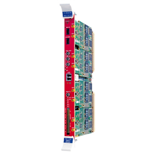

8 Channel 14 bit 100 MS/s Digitizer
The VX1724 is a digitizer able to record waveforms along with performing advanced algorithms for online digital pulse processing (DPP) of pulse height analysis and dynamic acquisition window.
Data is read by a Flash ADC, 14-bit resolution and 100 MS/s sampling rate, which is well suited for high-resolution detectors as Silicon, HPGe or inorganic scintillators like NaI or CsI coupled with Charge Sensitive Preamplifiers. In the waveform recording mode, algorithms of zero suppression are also implemented to reduce the data throughput. The acquisition can be channel independent and it is possible to make coincidence/anti-coincidence logic among different channels and external veto/gating. Multiple boards can be synchronized to build up complex systems.
In the case of DPP mode, data can be saved in time-stamped list mode to support higher input rates and improve the throughput performances. Piled-up events can be rejected or saved for offline analysis. The acquisition in DPP-PHA mode is fully controlled by the CoMPASS and MC2Analyzer software, which manage the algorithm parameters, build the plots and saves the relevant energy and time spectra. In the case of waveform recording mode, the user can take advantage of the CAENScope and WaveDump software to access and save the waveforms. For DPP-DAW mode, a c demo fully controls the acquisition, data plotting and saving.
Libraries and demo software in C and LabView are available for integration and customization of specific acquisition systems.
The VX1724 comes in a VME64X form factor with 8 input channels. The communication to and from the board is provided through the VMEBus and Optical Link interfaces.
Channels:8 channels single-ended
Bandwidth: 40 MHz
Impedance: 50 Ω
Connector: MCX
Full-Scale Range: 2.25 Vpp (default) 0.5 Vpp and 10 Vpp (on request)
Offset: Programmable DAC for DC offset adjustment in the full range
Abs Max Rating: @2.25 Vpp: 6 Vpp (with Vrail max +6 V or –6 V for any DAC offset value)
Resolution: 14 bits
Sampling Rate:
100 MS/s simultaneously on each channel
16.1 MS/s minimum by hardware down-sampling (see AN6308)
781 kS/s minimum by firmware decimation (Waveform recording firmware only)
ENOB: 11.89 (64 kS Buffer)
SINAD: 73.85 dB
THD: 87.8 dB
SFDR: 93.5 dB
SIGMA: 1.09 LSB rms (64 kS buffer, open input)
Clock source: internal/external
Onboard programmable PLL provides generation of the main board clocks from an internal (50 MHz local Oscillator) or external (front panel CLK-IN connector) reference
One Altera Cyclone EP1C20 per channel
12 bit / 100 MHz DAC FPGA controlled output with five operating modes:
4.5 A @ +5 V
200 mA @ +12 V
200 mA @ -12 V
Compare with Digitizers.
Loading...
| Code | Description |
|---|---|
| WVX1724BXAAA | VX1724B - 8 Ch. 14 bit 100 MS/s Digitizer: 4MS/ch, C4, SE (Obsolete) |
| WVX1724CXAAA | VX1724C - 8 Ch. 14 bit 100 MS/s Digitizer: 512KS/ch, C4, DIFF (Obsolete) |
| WVX1724DXAAA | VX1724D - 8 Ch. 14 bit 100 MS/s Digitizer: 4MS/ch, C4, DIFF (Obsolete) |
| WVX1724EXAAA | VX1724E - 8 Ch. 14 bit 100 MS/s Digitizer: 4MS/ch, C20, SE RoHS |
| WVX1724FXAAA | VX1724F - 8 Ch. 14 bit 100 MS/s Digitizer: 4MS/ch, C20, DIFF (Obsolete) |
| WVX1724XAAAA | VX1724 - 8 Ch. 14 bit 100 MS/s Digitizer: 512KS/ch, C4, SE (Obsolete) |
Desktop single-slot VME64X Crate
VME to USB 3.0/Ethernet/Optical Link Bridge
VME64 to USB 2.0/Optical Link Bridge
9U 21Slot VME64X Enhanced Crate series
8U 21 Slot VME64/64X Enhanced Crate Series
7U 21 Slot VME64 Low Cost Crate
7U 21 Slot VME64 Low Cost Crate
4U 8 Slot VME64X Mini Crate
4U 8 Slot VME64 Mini Crate
2U 4 Slot VME64X Mini Crate
2U 4 Slot VME64 Mini Crate
7U CRATE VME/NIM 8 slot VME64 365W, 5 slot NIM 150W
PCI Express Gen 3 CONET2 Controller
USB 3.0 to CONET2 Adapter
CAEN Digitizer readout application
Graphical software tool for digitizers running DPP-PHA firmware
Multiparametric DAQ Software for Physics Applications
Digitizer Software for Signal Inspection and Waveform Recording
Multi-Functional Software Suite for the Upgrade of Front-end Boards, Bridges and Power Supplies
+39 0584 388 398
Contacts
What are you looking for?
Search