

3 Years Warranty

4/8 Channel 10 bit 2/1 GS/s Digitizer
The CAEN Mod.VX1751 is a digitizer able to record waveforms along with performing advanced algorithms for online digital pulse processing (DPP) of charge integration and pulse shape discrimination with constant fraction timing and zero-length encoding.
Data is read by a Flash ADC, 10-bit resolution and 1 GS/s sampling rate (2 GS/s using half of the channels in DES mode*), which is well suited for fast signals as the ones coming from fast organic, inorganic and liquid scintillators coupled to PMTs or Silicon Photomultipliers, Diamond detectors and others. The acquisition can be channel independent and it is possible to make coincidence/anti-coincidence logic among different channels and external veto/gating. Multiple boards can be synchronized to build up complex systems.
In the case of DPP mode, data can be saved in time-stamped list mode to support higher input rates and improving the throughput performances.
Piled-up events can be rejected or saved for offline analysis. The acquisition in DPP mode is fully controlled by the CoMPASS software, which manages the algorithm parameters, builds, plots and saves the relevant energy, time, and PSD spectra. In the case of waveform recording mode, the user can take advantage of the CAENScope and WaveDump software to access and save the waveforms.
Libraries and demo software in C and LabView are available for integration and customization of specific acquisition systems.
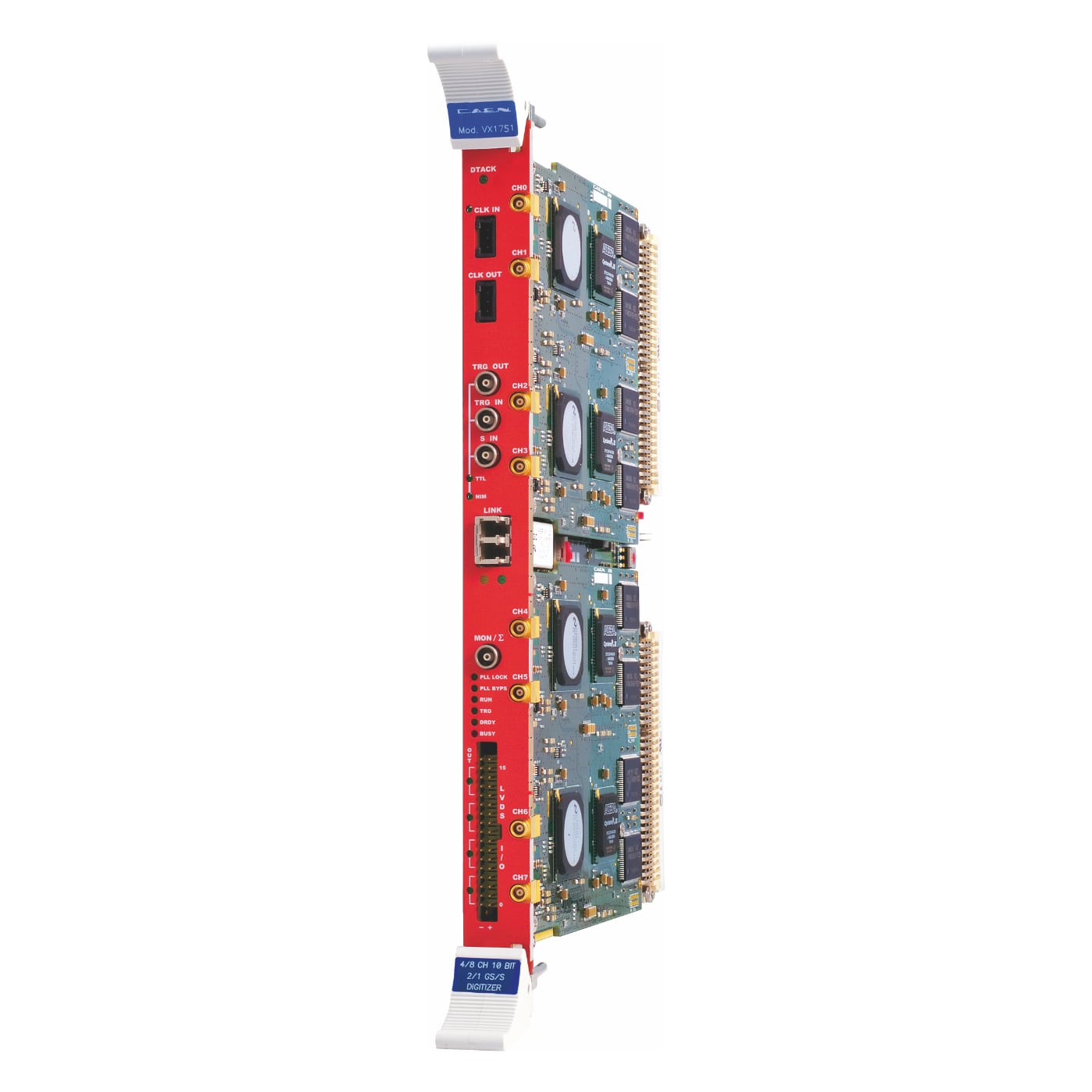
The VX1751 comes in a VME64X form factor with 4/8 input channels (4 channels in case of DES mode*). The communication to and from the board is provided through the VMEBus and Optical Link interfaces.
(*) NOTE: DES mode is not available with DPP firmware
Form Factor: 1-unit wide, 6U VME64X
Weight: 535 g
Channels: 8/4 channels single-ended
Bandwidth: 500 MHz
Impedance: 50 Ω
Connector: MCX
Full-Scale Range: 1 Vpp (default); 0.2 Vpp (on request)
Offset: Programmable DAC for DC offset adjustment in the full range
Abs Max Rating: @1 Vpp: 3 Vpp (with Vrail max +3 V or –3 V for any DAC offset value)
@200 mVpp: 2 Vpp (with Vrail max +2 V or –2 V for any DAC offset value)
Resolution: 10 bits
Sampling Rate:
1 GS/s (2 GS/s in DES mode)
Simultaneously on each channel
250 MS/s minimum by hardware down-sampling (see AN6308)
ENOB: 9.04 (56 kS Buffer)
SINAD: 56.19 dB
THD: 70.2 dB
SFDR: 79.7 dB
SIGMA: 0.58 LSB rms (56 kS buffer, open input)
Clock source: internal/external
Onboard programmable PLL provides generation of the main board clocks from an internal (50 MHz local Oscillator) or external (front panel CLK-IN connector) reference
1.835 MS/ch (1.9 ms @ 1GS/s) or 3.6 MS/ch in DES mode (1.9 ms @ 2GS/s); 14.4 MS/ch (15 ms @ 1 GS/s) or 28.8 MS/ch in DES mode (15 ms @ 2 GS/s) divisible into 1 ÷ 1024 buffers
Independent read and write access
Programmable event size and pre/post-trigger
Four Altera Cyclone EP3C16 (one FPGA serves 2 channels)
Libraries: General-purpose C and LabVIEW Libraries
Readout Software: CAEN WaveDump, CAENScope, CoMPASS, DPP-ZLEplus Demo software
Configuration Tools: CAEN Upgrader for Firmware upgrade, Direct Register R/W, Example codes
6.5 A @ +5V; 200 mA @ +12V, 300 mA @ -12V
Compare with Digitizers.
Loading...
| Code | Description |
|---|---|
| WVX1751BXAAA | VX1751B - 4/8 Ch. 10 bit 2/1 GS/s Digitizer: 3.6/1.8MS/ch, EP3C16, DIFF (Obsolete) |
| WVX1751CXAAA | VX1751C - 4/8 Ch. 10 bit 2/1 GS/s Digitizer: 28.8/14.4MS/ch, EP3C16, SE RoHS |
| WVX1751XAAAA | VX1751 - 4/8 Ch. 10 bit 2/1 GS/s Digitizer: 3.6/1.8MS/ch, EP3C16, SE RoHS |
Desktop single-slot VME64X Crate
VME to USB 3.0/Ethernet/Optical Link Bridge
VME64 to USB 2.0/Optical Link Bridge
9U 21Slot VME64X Enhanced Crate series
8U 21 Slot VME64/64X Enhanced Crate Series
4U 8 Slot VME64X Mini Crate
2U 4 Slot VME64X Mini Crate
PCI Express Gen 3 CONET2 Controller
USB 3.0 to CONET2 Adapter
Open Source Software for Digitizer 2.0 and 1.0 Series
CAEN Digitizer readout application
Multiparametric DAQ Software for Physics Applications
Firmware Upgrade Tool for Front-end Boards Bridges & VME Power Supply
Multi-Functional Software Suite for the Upgrade of Front-end Boards, Bridges and Power Supplies
Digital Pulse Processing for the Zero Length Encoding
Super Licence for CAEN Digitizers
Digital Pulse Processing for Charge Integration and Pulse Shape Discrimination
Digitizer Waveform Recording Firmware
+39 0584 388 398
Contacts
What are you looking for?
Search