

3 Years Warranty

16/8 Channel 14-bit 250 MS/s Digitizer
The CAEN Mod. V1725S is a digitizer capable of recording waveforms along with performing advanced algorithms for online digital pulse processing (DPP). Utilizing DPP Firmware, users can acquire quantitative physical parameters (Integrated Charge, Pulse Shape Discrimination with very fine time resolution, Pulse Height Analysis) as well as read out waveforms with automatic pulse identification and baseline suppression on channel basis (Zero-Length Encoding and Dynamic Acquisition Window). The wide range of DPP algorithms supported by the V1725S make it a “must-have” for any type of nuclear physics application.
The V1725S (previously V1725) has also been upgraded, introducing a larger FPGA to accommodate more complex DPP algorithms and a new A/D converter for better stability which does not require temperature-related calibration.
Input signals are read by a Flash ADC, 14-bit resolution and 250 MS/s sampling rate, which is well suited for mid-fast signals as the ones coming from liquid or inorganic scintillators coupled to PMTs or Silicon Photomultipliers, but also for high precision detectors as Silicon or HPGe coupled with charged sensitive preamplifiers. The acquisition can be channel independent and it is possible to make coincidence/ anti-coincidence logic among different channels and external veto/gating. Multiple boards can be synchronized to build up complex systems. In the case of DPP mode, data can be saved in time-stamped list mode to support higher input rates and improving the throughput performances. Piled-up events can be rejected or saved for oine analysis. The acquisition in DPP mode is fully controlled by the CoMPASS software, which manage the algorithm parameters, build the plots and saves the relevant energy, time, and PSD spectra. In case of waveform recording mode, the user can take advantage of the CAENScope and WaveDump software to access and save the waveforms. Libraries and demo software in C and LabView are available for integration and customization of specific acquisition systems.
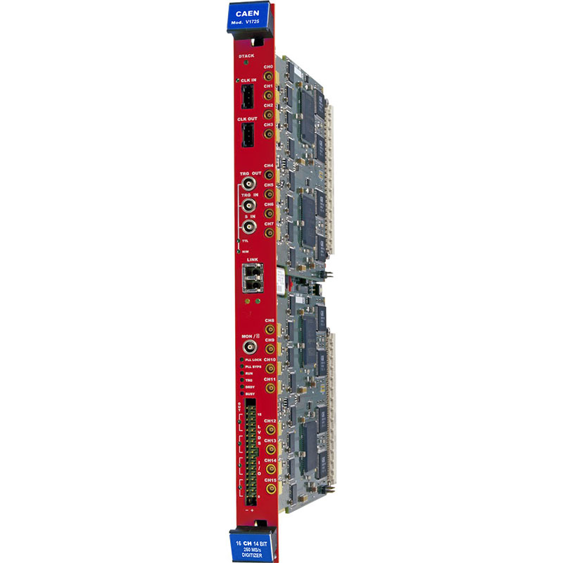
The V1725S family comes in a VME form factor, with 16/8 input channels. The communication to and from the board is provided through the VMEBus and Optical Link interfaces.
The V1725 fits in the single-slot CAEN VME64X u-crate, which allows you to convert the VME digitizer into a desktop board for lab tests.
This product is compatible with the following third-party software:
Form Factor: 1-unit wide, 6U VME64
Channels: 16/8 channels single ended
Bandwidth: 125 MHz
Impedance: 50 Ω
Connector: MCX
Full Scale Range: 0.5 or 2 Vpp (SW selectable)
Offset: Programmable DAC for DC offset adjustment in the full scale range
Resolution: 14 bits
Sampling Rate: 250 MS/s Simultaneously on each channel
V1725Sx Baseline RMS Noise (open inputs)
@ 2 Vpp: 2.6 LSB = 312 uV
@ 0.5 Vpp: 3.4 LSB = 102 uV
Clock source: internal/external
Onboard programmable PLL provides generation of the main board clocks from an internal (50 MHz local Oscillator) or external (front panel CLK-IN connector) reference
12-bit/125 MHz DAC FPGA controlled output with four operating modes:
Waveform Recording Firmware: Free firmware for waveform recording
Upgrades: Firmware can be upgraded via Optical Link or VMEBus
DPP Firmware: Paid firmware for Digital Pulse Processing: DPP-PSD, DPP-PHA, DPP-ZLEplus, and DPP-DAW
VX1725: 5.2 A @ +5 V; 750 mA @ +12 V; -12 V not used
V1725S: 7.5 A @ +5 V; 700 mA @ +12 V; -12 V not used
V1725SB: 8 A @+5V; 800 mA @+12V; -12V not used
V1725SC: 5 A @+5V; 500 mA @+12V; -12V not used
V1725B/1725C/1725D: n.a.
V1725SD: 6.5 A @ +5 V; 500 mA @ +12 V; -12 V not used
Compare with Digitizers.
Loading...
| Code | Description |
|---|---|
| WV1725BXAAAA | V1725B - 16 Ch. 14 bit 250 MS/s Digitizer: 5.12MS/ch, CE30, SE (Obsolete) RoHS |
| WV1725CXAAAA | V1725C - 8 Ch. 14 bit 250 MS/s Digitizer: 640kS/ch, CE30, SE (Obsolete) RoHS |
| WV1725DXAAAA | V1725D - 8 Ch. 14 bit 250 MS/s Digitizer: 5.12MS/ch, CE30, SE (Obsolete) RoHS |
| WV1725XAAAAA | V1725 - 16 Ch. 14 bit 250 MS/s Digitizer: 640kS/ch, CE30, SE (Obsolete) RoHS |
| WV1725SBXAAA | V1725SB - 16 Ch. 14 bit 250 MS/s Digitizer: 5.12MS/ch, Arria V GX, SE RoHS |
| WV1725SCXAAA | V1725SC - 8 Ch. 14 bit 250 MS/s Digitizer: 640kS/ch, Arria V GX, SE RoHS |
| WV1725SDXAAA | V1725SD - 8 Ch. 14 bit 250 MS/s Digitizer: 5.12MS/ch, Arria V GX, SE RoHS |
| WV1725SXAAAA | V1725S - 16 Ch. 14 bit 250 MS/s Digitizer: 640kS/ch, Arria V GX, SE RoHS |
Desktop single-slot VME64X Crate
9U 21Slot VME64X Enhanced Crate series
8U 21 Slot VME64/64X Enhanced Crate Series
7U 21 Slot VME64 Low Cost Crate
7U 21 Slot VME64 Low Cost Crate
4U 8 Slot VME64X Mini Crate
2U 4 Slot VME64 Mini Crate
VME to USB 3.0/Ethernet/Optical Link Bridge
VME to USB 2.0 / Optical Link Bridge
7U CRATE VME/NIM 8 slot VME64 365W, 5 slot NIM 150W
Clock Generator and FAN-OUT
PCI Express Gen 3 CONET2 Controller
USB 3.0 to CONET2 Adapter
CAEN Digitizer readout application
Multiparametric DAQ Software for Physics Applications
Library of functions for CAEN Digitizers high level management
Interface library for CAEN Data Acquistion Modules
Multi-Functional Software Suite for the Upgrade of Front-end Boards, Bridges and Power Supplies
Digital Pulse Processing for the Zero Length Encoding
Super Licence for CAEN Digitizers
Digital Pulse Processing for Charge Integration and Pulse Shape Discrimination
Digital Pulse Processing for the Pulse Height Analysis
Digital Pulse Processing with Dynamic Acquisition Window
Digitizer Waveform Recording Firmware
+39 0584 388 398
Contacts
What are you looking for?
Search