Logo Caen

V2740

New

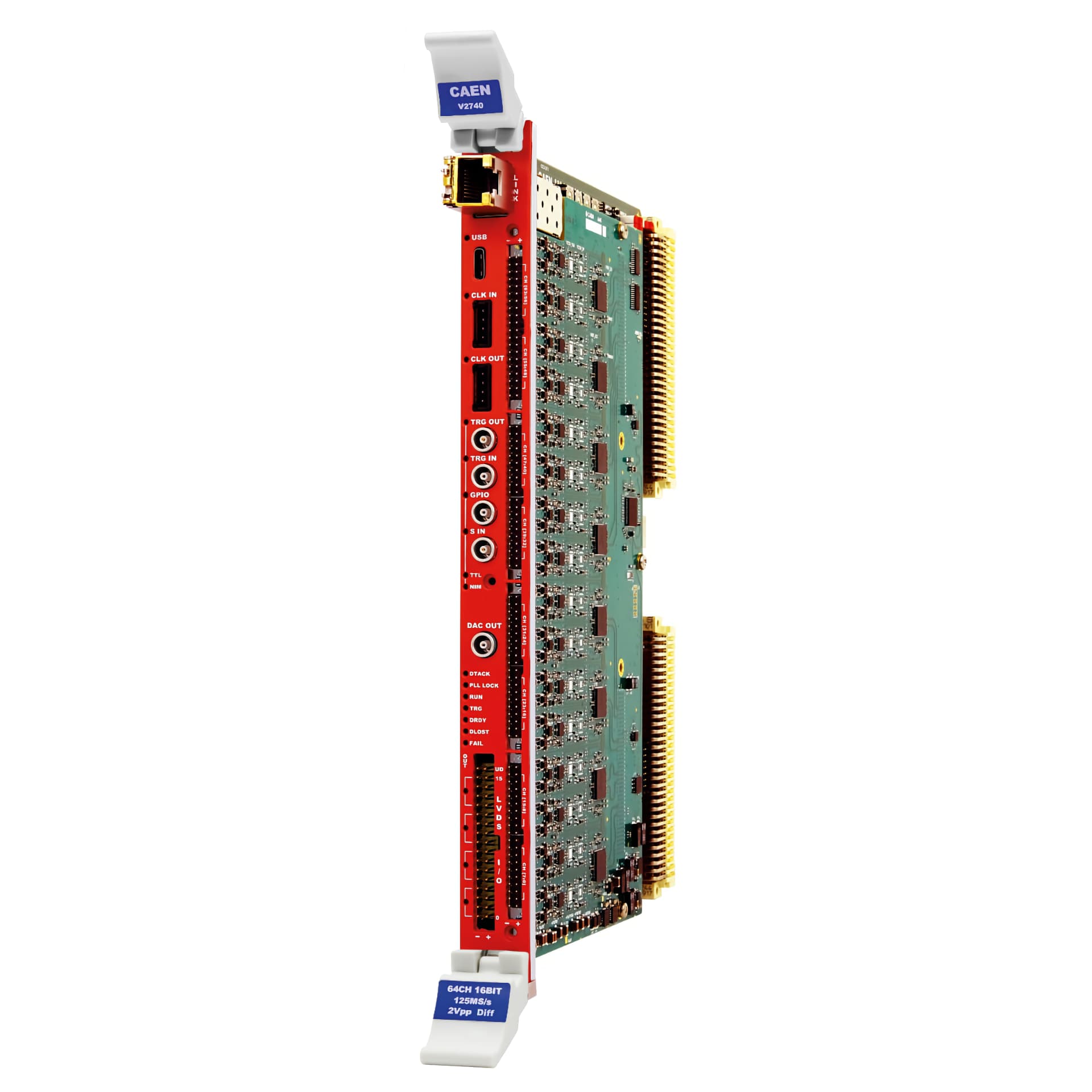
64 Channel 16 bit 125 MS/s Digitizer

Features

  • 16 bit @ 125 MS/s ADC
  • 64 analog inputs, differential or single-ended, on four 2mm 40-pin header connectors
  • 2Vpp input range, fixed Analog Gain x1
  • DT2740 desktop form factor also available
  • Open FPGA programming through graphical tool SCI-Compiler
  • Wide range of applications (from Neutrino Physics & Dark Matter to Nuclear and Particle Physics to Spectroscopic Imaging)
  • Suited for signals from Semiconductor Detectors coupled with CSPs (Si, HPGe) or scintillators coupled with PMTs (NaI, CsI)
  • On-board firmware selection for different acquisition modes:
    • Scope mode (simultaneous raw waveform acquisition on common trigger)
    • DPP-PHA mode (pulse height and time acquisition on independent channel self-triggers)
    • DPP-PSD mode (pulse shape discrimination and time acquisition on independent channel self-triggers)
    • Predisposition for other algorithms like zero suppression and data reduction
  • Multi-board synchronization and system building capabilities
  • Front panel fully programmable I/Os (4 LEMO TTL/NIM and 16 LVDS)
  • Special 125 MS/s 14bit DAC output (LEMO) for signal inspection, pulse generation, majority level
  • 2.5GB of Total Acquisition memory (DDR4)
  • On-board Zynq® UltraScale+™ MPSoC integrating an Arm®-based CPU running Linux®
  • Multi Interface: USB-3.0 and 1/10 GbE or CONET Available on request optical link (switchable on the same socket)
  • SDK for embedded Arm and host PC
  • Open FPGA architecture for pulse analysis algorithm customization

Overview

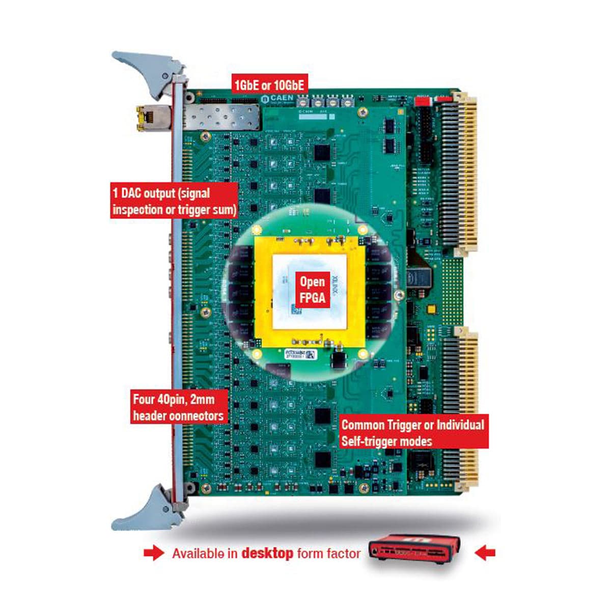
The CAEN Mod.V2740 Digitizer is a 64-channel digital signal processor for radiation detectors in a VME64 form factor. It offers not only waveform digitization and recording but also Multi-Channel Analysis for nuclear spectroscopy using Silicon strip, segmented HPGe, Scintillation detector with PMTs, Wire Chambers, and others.

Independently for each of the 64 channels, the V2740 can perform pulse height measurements (PHA), and other algorithms that will be gradually developed, such as constant fraction timing (CFD) and pulse shape discrimination (PSD).
Each channel of the module digitizes the analog input, that can be the signal coming from a physics detector, with a 16 bit, 125 MS/s ADC. The sampled data are used to initiate the digital pulse processing sequence, managed in the FPGA at the firmware level. Different firmware types can be selected via software, according to the specific setup and acquisition mode.

  • Common trigger: all channels acquire simultaneously with a common trigger. The trigger can be fed externally or generated by a combination of individual channel discriminators. This mode is mainly intended for the acquisition of waveforms, like a digital oscilloscope. Options for zero suppression are available to remove not significant data.
  • Independent trigger: suited for trigger-less applications, where no global trigger is needed but each channel acquires waveforms upon its self-trigger which fires through a digital discriminator, independently of the others.
  • DPP: real-time processing in the FPGA allows for the extraction of physical parameters from the waveform (e.g. pulse height, charge, timestamp, PSD), well suited for high counting rate applications. It is yet possible to save both raw waves and parameters.

A template of the firmware is available for customers who want to personalize the acquisition to implement custom algorithms for pulse processing in the open FPGA. The user can have control of the data output information and customize the trigger logic to get several combinations of self-triggers and I/O signals to validate or discard the events.
Custom software can run on the onboard CPU for data reduction and analysis. Multi-board synchronization can be implemented via backplane or front panel easy-cabling options.
The communication interface selection offers fast readout options: USB 3.0 type-C and 1/10 Gigabit Ethernet or optional Optical (CONET – CAEN Daisy Chainable Optical Link Protocol Available on request) Links.

For detailed information on available firmware for the 2740 family and the structure of programming files (.CUP), please refer to the following page.

The V2740 fits in the single-slot CAEN VME64X u-crate, which allows you to convert the VME digitizer into a desktop board for lab tests. Moreover, you can check this FAQ to see which CAEN VME crates are suitable for this product.

Supported third-party software:

Technical Specifications

GENERAL

Form Factor: 1-unit wide, 6U VME64
Weight: 642 g Valid also for B versions
Dimension: 6U x 160 mm

ANALOG INPUT

Channels: 64 channels, differential on 2740, single-ended on 2740B versions
Impedance: differential: 100 Ω, single-ended: 50 Ω  (10 kΩ  personalization available)
ICMR (Input Common-Mode Range): ± 8 Vdc referred to Gnd (Differential mode only)
Full Scale Range: 2 Vpp
Gain: fixed x1
Bandwidth (-3dB): 50 MHz
DC Offset: Adjustable in the ± 1.25V range independently on each channel
Connector Type: Four 2mm 40-pin header male; input adapters available

DIGITAL CONVERSION

Resolution: 16 bits
Sampling Rate: 125 MS/s simultaneously on each channel. Scalable by 2n decimation factor, n = 1 to 10 (Scope firmware only)

PERFORMANCE

ENOB: 11.7 (Typ.)
RMS: 3.9 LSB (≃ 120 µV) typical RMS

DIGITAL I/O
CLK-IN, CLK-OUT

  • Two different pairs:
    o CLK, reference clock signal
    o SYNC, synchronization signal (start/stop, T0, etc.)
  •  2.54mm, 4-pin AMPMODU Mod II male connector
  • CLK-IN: AC-coupled LVDS, ECL, PECL, LVPECL, CML (Zdiff = 100 Ω)
  • CLK-OUT: LVDS
  • Daisy chainable for multiboard synchronization with sw programmable CLK-OUT delay shift
LVDS I/O

  • 16 differential pairs
  • Software programmable I/O (individual self-trigger outputs, trigger validations, Veto, Busy, Start, Stop, Pattern Input, etc.)
  • LVDS
  • Zdiff = 100 Ω (when set as inputs)
  • 2.54mm 34-pin AMPMODU Mod II male connector
TRG-IN/TRG-OUT/GPIO/S-IN

General purpose I/Os
Software programmable (trigger, gate, veto, busy, etc.)
Sigle-ended TTL/NIM

  • TRG-IN/S-IN internally terminated with 50 Ω (Zin = 50 Ω)
  • TRG-OUT requires Rt = 50 Ω
  • GPIO as Input must be terminated with 50 Ω
  • GPIO as TTL Output requires Rt = 50 Ω
  • GPIO as NIM Output requires Rt = 50 Ω or 25 Ω

LEMO 00 male connector


DAC OUT
  • DAC output for signal inspection, pulse generation, majority level
  • 14-bit Digital-to-Analog Converter (DAC)
  • 125MS/s Update Rate
  • ±1 V @ 50 Ω load; ±2 V @ hi-Z load Output Range
  • LEMO 00 male connector
ACQUISITION MEMORY

2.5 GB total DDR4 memory size (20.971 MS/ch) divisible in multiple buffers
Maximum record length: ≃ 84 ms @ 125 MS/s (total memory size divided by 2)1

1 Value referred to the Scope firmware (minimum of two buffers admitted)

TRIGGER
Modes

  • Common: all channels acquire simultaneously with the trigger (software, external or logic combination of self-triggers)
  • Individual: each channel acquires independently with its self-trigger
  • Correlated: the individual self-trigger of each channel is validated by the coincidence/anticoincidence logic between other self-triggers and/or external I/Os
Trigger Time Stamp

Resolution: 8 ns coarse time stamp, 8ps fine time stamp (DPP firmware only)
Counter range: 48 bits
Full-scale range: ~625 h

SYNCHRONIZATION
Clock Propagation

Typical 62.5MHz frequency distributed:

  • By fan-out to CLK-IN
  • By daisy chain through CLK-IN/CLK-OUT

Custom frequencies can be supported

Acquisition Start/Stop

Daisy chain or fan-out propagation through CLK-IN/CLK-OUT or NIM/TTL, LVDS I/Os


Data Sync 

Busy/Veto logic on LVDS I/Os or NIM/TTL I/Os for event building synchronization

Trigger Distribution

TRG-IN/TRG-OUT NIM/TTL LEMO I/Os (common trigger) or LVDS I/Os (common or individual trigger)

Trigger Time Stamp Reset

Software from START run command or Hardware from S-IN/GPIO input (Scope Firmware only)

FIRMWARE

Firmware stored in the on-board Flash Memory and live rebootable by Web Interface
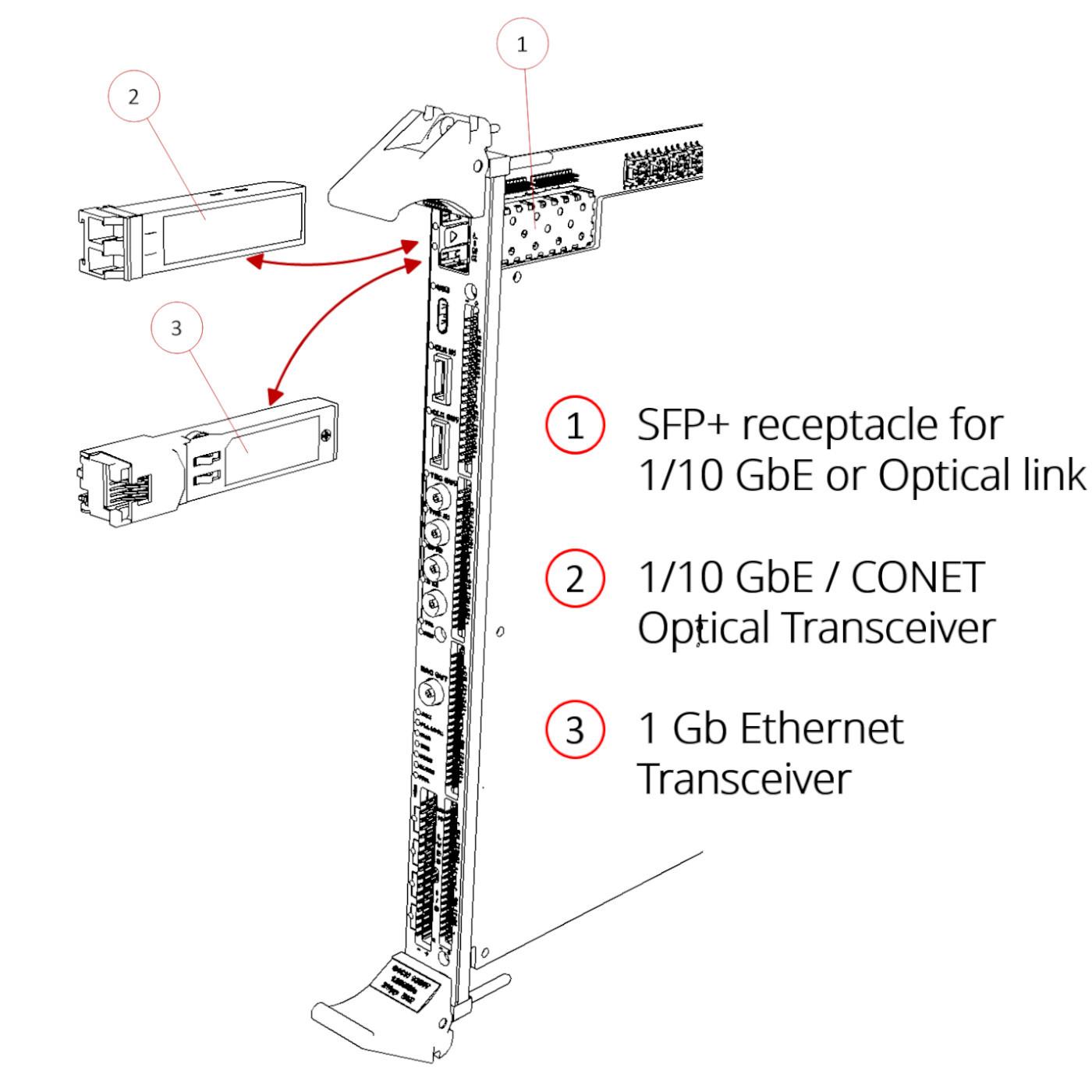
DPP Firmware

Implements the digital pulse processing algorithm:

  • DPP-PHA: Pulse Height Analysis
  • DPP-PSD: Pulse Shape Discrimination
  • DPP-ZLE: Zero Length Encoding  
  • DPP-DAW: Dynamic Acquisition Window coming soon
Upgrades

Any supported firmware can be uploaded via Web Interface (both different firmware types and upgraded versions of the same firmware)

Scope Firmware

Firmware for the waveform recording


FPGA
  • Xilinx Zynq UltraScale+ Multiprocessor System-on-Chip mod. XCZU19EG
  • Processing System based on Quad-core Arm with 2GB DDR4 memory @2400 MT/s (Linux OS onboard)
  • Programmable logic with more than 1100K system logic cells and 80Mbit memory
OPEN FPGA
User-Scope Template

Common trigger, simultaneous waveform recording on 64 channels management. Trigger logic and wave processing customization

User-DPP Template

Individual trigger and channel acquisition management. Customization of DPP algorithm, trigger logic, and event data information

COMMUNICATION INTERFACE
1 GbE

  • Copper RJ45 or optical LC connector on SFP+ transceiver
  • Protocol: TCP
  • Transfer rate: 110 MB/s


10 GbE (Available on Request)

  • Copper RJ45 or LC optical connector on SFP+ transceiver
  • Protocol: TCP/IP, UDP
  • Transfer rate: 280 MB/s (TCP/IP), t. b. d. (UDP)
CONET (Available on Request)

  • Optical LC connector on SFP+ transceiver
  • CONET2 protocol (CAEN proprietary)
  • Transfer rate: 80 MB/s


USB 3.0

  • USB-C type connector
  • Protocol: USB 3.1 GEN1
  • Transfer rate: 280 MB/s
SOFTWARE

Readout SW
– CoMPASS spectroscopy software (for DPP firmware only)
– WaveDump2 (for Scope firmware only)

SDK and Tools
General purpose C libraries with demo samples for host Windows® and Linux® PC, and embedded Arm processor

SCI-Compiler (Open FPGA)
Automatic generation of drivers (USB, ethernet), libraries, and demo software for Windows®, Linux®

Web Interface
Firmware management (e,g. upgrades and on-the-fly selection of the firmware to run), board information, PLL and Ethernet configuration, board status monitoring

POWER REQUIREMENTS

+12V: 1.1 A (Typ.)
+5V: 6.2 A (Typ.)

Compare

Compare with Digitizers.

Loading...

Accessories

A372F
64 channel 2.54mm Male Header Connector Adapter for 274x Digitizers
A372M
64 channel MCX Coax Connector Adapter for SE signals
A319A
Clock & Sync cable assembly for Digitizer Series 2.0 - 20 cm
A319B
Clock cable assembly from Digitizer Series 1.0 to Digitizer Series 2.0 - 20cm
A316
Cable assembly 2.54mm 2-pin header female - 5 cm
A952
Cable assembly 2.54mm 34 pin female to 2.54mm 34 pin female - 50 cm
A953
Cable assembly 2.54mm 34 pin female to two 2.54mm 34 pin female – 50 cm
A954
Cable assembly 2.54mm 34 pin female to two 2.54mm 16 pin female - 50 cm

Ordering Options

Code Description
WV2740XAAAAA V2740 - 64 Ch 16 bit 125MS/s Digitizer, Diff   RoHS
WV2740BXAAAA V2740B - 64 Ch. 16 bit 125 MS/s Digitizer, SE   RoHS

Contacts

Great to have you back!