

3 Years Warranty

32+2 Channel 12bit 5 GS/s Digitizer
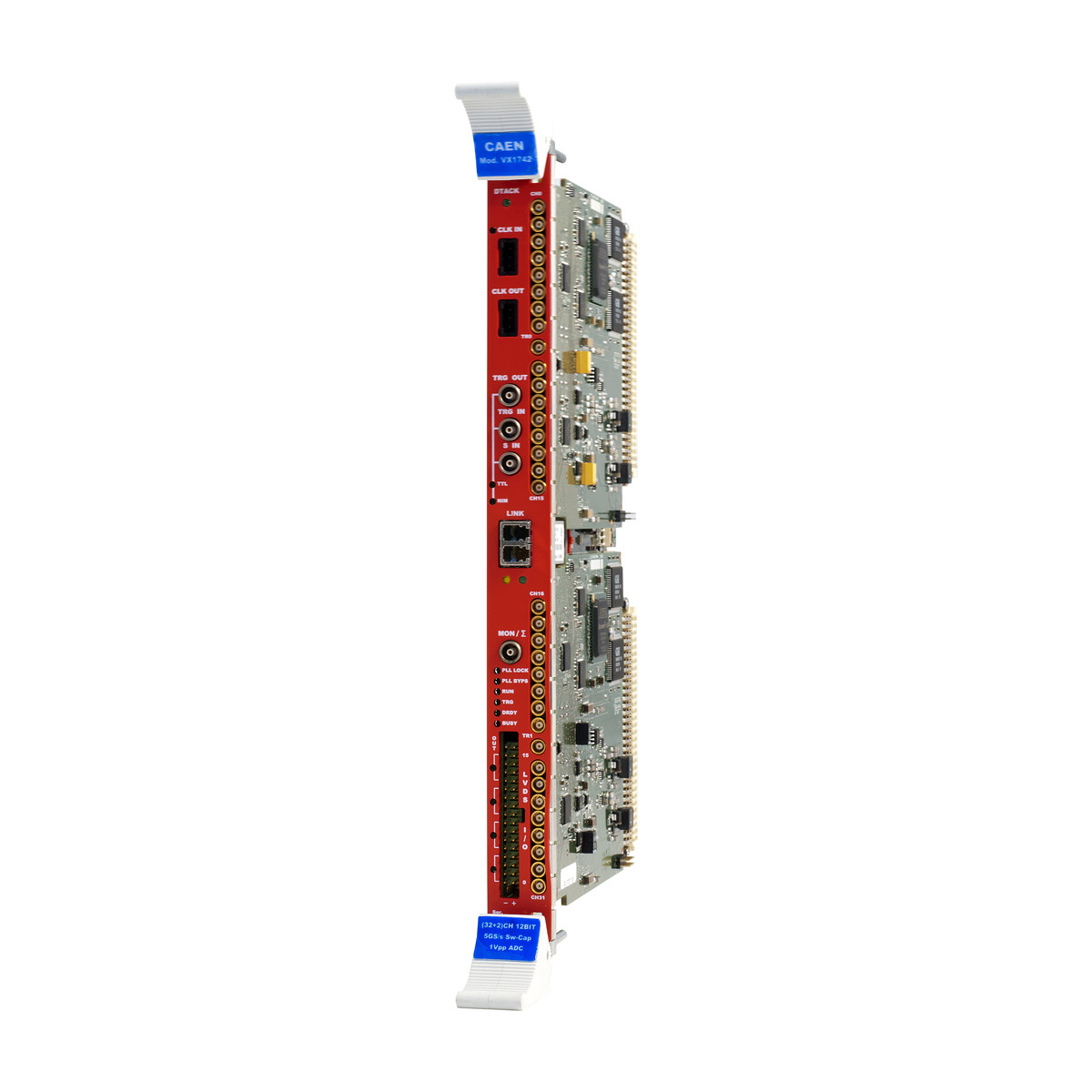
The CAEN Mod. VX1742 is a 1-unit wide VME64X board housing 32+2 Channel 12 bit 5 GS/s Switched Capacitor Digitizer sections. The input dynamic range is 1 Vpp on single-ended MCX coaxial connectors (16-bit DAC on each channel to control the DC Offset).
The digitizer is based on the Switched Capacitor Array DRS4 chip (Domino Ring Sampler). This technology relies on a series of 1024 capacitors (analog memory) in which the analog input signal is continuously sampled in a circular way.
The sampling frequency is 5 GHz by default and it can be programmed to 2.5 GHz, 1GHz, and 750 MHz. The analog to digital conversion is not simultaneous with the chip sampling phase, and it starts as soon as the trigger condition is met, thus producing a dead time of 110 μs in case only the analog inputs are digitized, 181 μs when also the fast trigger TRn is digitized. When the trigger stops the DRS4 chip sampling (holding phase), the analog memory buffer is frozen, and the cell content is made available to the 12 bit ADC for the digital conversion.
The digital memory allows to store subsequent events, even if the readout is not yet started. Moreover, since the digital memory buffers work like FIFOs, the readout activity from VME or Optical Link does not affect write operations of subsequent events.
The available trigger sources are:
The module features the front panel CLK IN/CLK OUT connectors and an internal PLL for clock synthesis from internal/external references. V1742 supports multi-board synchronization allowing all DRS4s to be synchronized with a common clock source and ensuring Trigger Time Stamps alignment. Once synchronized, all data will be aligned and coherent across multiple V1742 boards.
The module is available with digital memory sizes of 128 event/ch or 1024 event/ch.
The VME interface of the module is VME64X compliant, and the data readout can be performed in several data transfer modes: BLT32, MBLT64 (up to 70 MB/s of transfer rate using CAEN Bridge), CBLT32/64, 2eVME, 2eSST (up to 200 MB/s of transfer rate). The built-in daisy chainable Optical Link is able to transfer data at 80 MB/s, thus it is possible to connect up to 8 boards to a single A4818 Controller, or up to 32 to a single A5818 Controller (4-link version).
Software available (Windows and Linux): CAEN provides drivers for all the different types of physical communication channels, a set of C and LabView libraries (CAENComm and CAENDigitizer), demo applications and utilities:
Software for V1742 running Waveform Recording Firmware:
The VX1742 fits in the single-slot CAEN VME64X u-crate, which allows you to convert the VME digitizer into a desktop board for lab tests.
Form Factor: 1‐unit wide VME64/VME64X boards
Weight: 520 g
Dimension: 6U x 160 mm
Channels: 32 channels, 2 special channel (TR0, TR1) Single ended
Full Scale Range (FSR): 1 Vpp
Absolute max analog input voltage: 3Vpp (with Vrail max +3V or ‐3V) for any DAC offset in single ended configuration
Impedance: Zin = 50 OhmDC Offset
Programmable 16-bit DAC for DC offset adjustment on each channel. Range ± 1 V
Connector: MCX
Bandwidth: 500 Mhz
Resolution: 12 bits
Switched Capacitor: Array Domino Ring Sampler chip (DRS4), 8+1 channels with 1024 storage cells each
Sampling Rate: 5 GS/s – 2.5 GS/s – 1 GS/s – 0.75 GS/s SW selectable, simultaneously on each channel
Dead Time (A/D Conversion): 110 μs, analog inputs only 181 μs, digitizing TR0
Altera Cyclone EP3C16 (one FPGA manages 16+1 channels)
Trigger Source
‐ Fast (Low Latency) trigger: Programmable threshold on TR0 and TR1 (each TRn signal drives two 8‐ch groups)
‐ Self‐trigger: Logic OR combination of channels over/under threshold (each channel self‐trigger drives two 8‐ch groups)
‐ External‐trigger: Common trigger by TRG‐IN connector
‐ Software‐trigger: Common trigger by software command
Trigger Propagation
TRG‐OUT programmable
digital output
Trigger Time Stamp
30‐bit counter (extendable to 60‐bit by sw)
8.5 ns resolution
9 s range
Timer reset by S‐IN
128 events/ch or 1024 events/ch Multi‐event buffer (1024 S/event, that is 200 ns/event @ 5 GS/s)
Independent read and write access
Programmable event size and pre/post‐trigger
Clock source: internal/external.
On‐board programmable PLL provides generation of the main board clocks from internal
(50 MHz local Oscillator) or external (front panel CLK‐IN connector) reference
|
Clock Propagation
Acquisition Synchronization
Trigger Time Stamps Alignment
Optical Link: CAEN CONET proprietary protocol, Up to 80 MB/s transfer rate, Daisy‐chain capability.
VME: VME 64X compliant. Data transfer mode: BLT32, MBLT64 (70 MB/s by CAEN Bridge), CBLT32/64, 2eVME, 2eSST (200 MB/s).
Waveform Recording Firmware: Free firmware for waveform recording
Upgrades: Supported via VMEbus/Optical Link
Readout SW: WaveDump readout software with C source files and VS project for developers (Windows® , Linux®)
Libraries and Tools: General purpose C libraries with readout demos (Windows® , Linux® , and LabVIEW™ support) and configuration tools
Environment: Indoor use
Operating Temperature: 0◦C to +40◦C
Storage Temperature: –10◦C to +60◦C
Operating Humidity: 10% to 90% RH non condensing
Storage Humidity: 5% to 90% RH non condensing
Altitude: < 2000m
Pollution Degree: 2
Overvoltage Category: II
EMC Environment: Commercial and light industrial
IP Degree: IPX0 Enclosure, not for wet location
EMC: CE 2014/30/EU Electromagnetic compatibility Directive
Safety: CE 2014/35/EU Low Voltage Directive
+12V 85mA
+5V 5,5A
Compare with Digitizers.
Loading...
| Code | Description |
|---|---|
| WVX1742BXAAA | VX1742B - 32+2 Ch. 12 bit 5GS/s Switched-Capacitor Digitizer: 1024 events/ch (1kS/event), EP3C16, SE RoHS |
| WVX1742XAAAA | VX1742 - 32+2 Ch. 12 bit 5GS/s Switched-Capacitor Digitizer: 128 events/ch (1kS/event), EP3C16, SE RoHS |
Desktop single-slot VME64X Crate
9U 21Slot VME64X Enhanced Crate series
8U 21 Slot VME64/64X Enhanced Crate Series
7U 21 Slot VME64 Low Cost Crate
7U 21 Slot VME64 Low Cost Crate
2U 4 Slot VME64 Mini Crate
1U 2 Slot VME64 Mini Crate
VME to USB 3.0/Ethernet/Optical Link Bridge
VME to USB 2.0 / Optical Link Bridge
7U CRATE VME/NIM 8 slot VME64 365W, 5 slot NIM 150W
PCI Express Gen 3 CONET2 Controller
USB 3.0 to CONET2 Adapter
CAEN Digitizer readout application
Library of functions for CAEN Digitizers high level management
Interface library for CAEN Data Acquistion Modules
Multi-Functional Software Suite for the Upgrade of Front-end Boards, Bridges and Power Supplies
Demo Software for x742 Digitizers Synchronization
Digitizer Waveform Recording Firmware
+39 0584 388 398
Contacts
What are you looking for?
Search