

3 Years Warranty
3 Years Warranty
3 Years Warranty
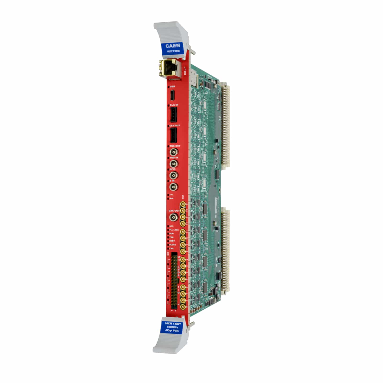

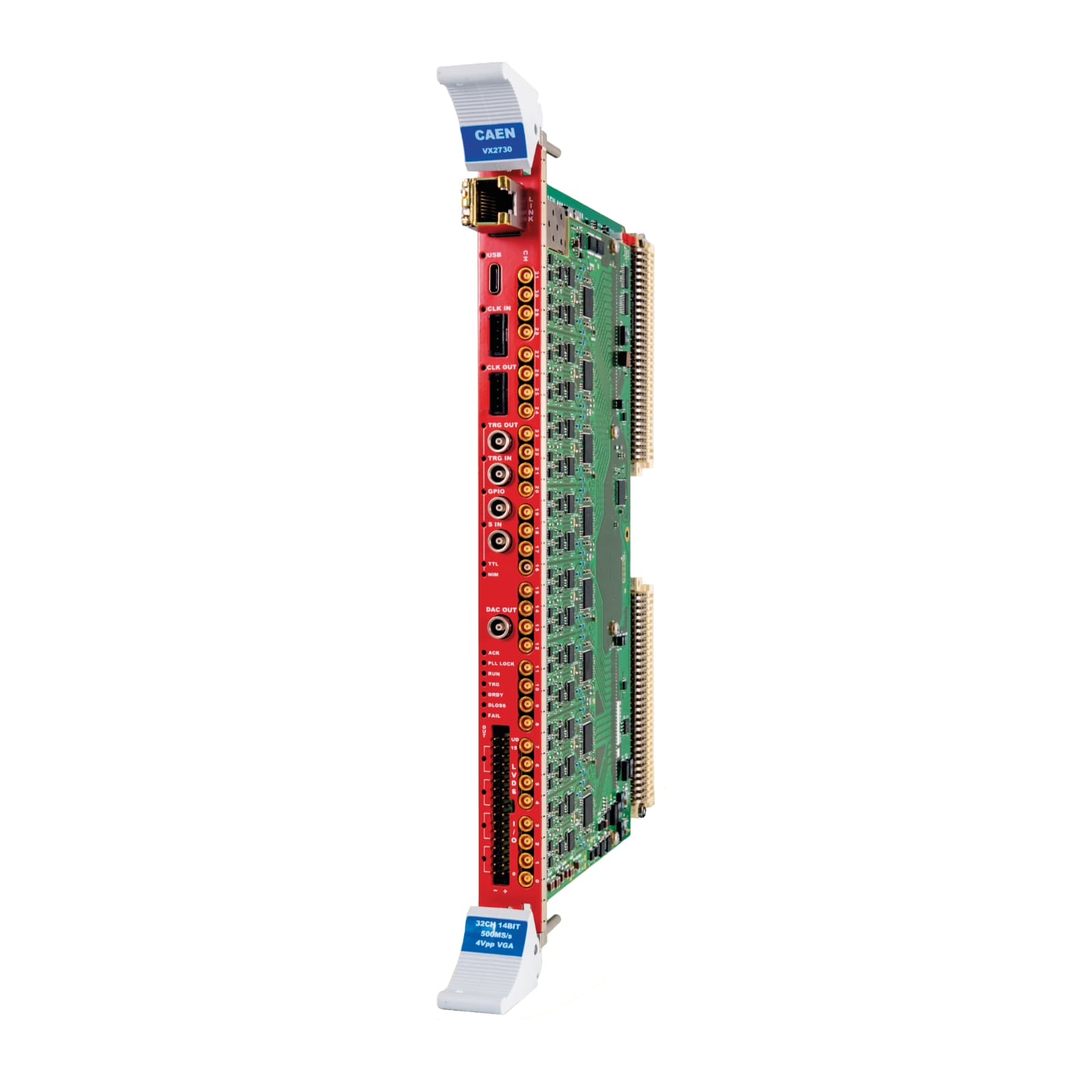
32/16 Channel 14 bit 500 MS/s Digitizer with programmable Input Gain
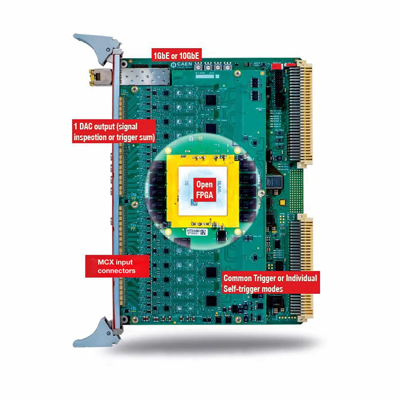
The VX2730 Digitizer is a 32/16-channel digital signal processor for radiation detectors in the VME64X form factor. It offers not only waveform digitization and recording but also Multi-Channel Analysis for a complete range of applications like nuclear and particle physics, high-timing resolution, Fast Neutron Spectroscopy, and Homeland Security. It is compliant with mid-fast signals typically coming from liquid or inorganic scintillators coupled to PMTs or SiPMs.
VX2730 features 32 or 16 (VX2730B) single-ended channels, each capable of digitizing detector signals using a 14-bit ADC at 500 MS/s. Data acquisition is driven by trigger signal generation and the identification of a Region of Interest (ROI), defined in terms of sample count or time duration. Trigger sources can be local (channel self-trigger), external, or software-based. Once acquired, the digitized data is processed within the FPGA, stored in high-speed memory as events—including Trigger ID and Timestamp tags—and then transferred via high-bandwidth communication interfaces for further analysis. The digitizer supports different acquisition modes, designed to balance throughput, latency, and data efficiency according to experimental requirements:
VX2730 can operate using both pre-configured firmware developed by CAEN and custom user-generated firmware, offering flexibility for a wide range of applications. Multiple firmware images can be stored simultaneously in the digitizer’s FLASH memory and quickly activated when needed. CAEN provides ready-to-use firmware solutions optimized for specific acquisition and processing needs:
The Linux-based Arm processor embedded in the onboard CPU makes it possible to run automated user routines. Multi-board synchronization can be implemented via backplane or front panel easy-cabling options. Multiple communication interfaces offer flexible readout options: USB 3.0 type-C and 1/10 Gigabit Ethernet.
For detailed information on available firmware for the 2730 family and the structure of programming files (.CUP), please refer to the following page.
The VX2730 fits in the single-slot CAEN VME64X u-crate, which allows you to convert the VME digitizer into a desktop board for lab tests. Moreover, you can check this FAQ to see which CAEN VME crates are suitable for this product.
This product is compatible with the following third-party software:
Weight: 700 g
Form Factor: 1-unit wide, 6U VMEX64
Dimension: 6U x 160 mm
Channels: 32/16 channels, single-ended
Bandwidth (-3dB): 250 MHz guaranteed for Gain ≥ 2
Impedance: 50 Ω
Gain: x1 ÷ x20, software programmable in steps of 1dB independently on each channel
Connector Type: MCX
Full Scale Range: 4 Vpp ÷ 0.2 Vpp
DC Offset: Adjustable in the ± 2.5V range independently on each channel
Resolution: 14 bits
Sampling Rate: 500 MS/s (simultaneously on each channel)
ENOB (Typ.): 10.5 (@50MHz, -3dB, Gain x2)
RMS (Typ.): 2.4 LSB RMS (@Gain x2)
|
(1) Value referred to the Scope firmware (minimum of two buffers admitted)
1 GbE
| 10 GbE (Contact CAEN Support)
| USB 3.0
|
Triggered: All channels fire simultaneously upon a global trigger generated by the Central Trigger Logic receiving the local trigger sources: Local (self-trigger), External, Software
Streaming readout: Each channel autonomously identifies the ROI. The channel’ self-trigger is used to start the acquisition and capture events independently of the other channels. Additionally, a correlated streaming mode validates events via coincidence/anticoincidence with local or external triggers
Software: By register writing
External: Upon the leading edge of TRG-IN signal (TTL/NIM)
Local (self-trigger): Upon the channel discriminator with programmable threshold
| Scope Firmware | DPP firmware | |
| Resolution | 8 ns coarse time stamp | 2 ns coarse timestamp / 2 ps fine time stamp |
| Counter range | 48 bits | 48 bits |
| Full-scale range | ~625 h | 156 h |
|
Developed by CAEN, stored in the on-board FLASH memory, and live rebootable by Web Interface
|
Sci-Compiler
User Firmware Generator and Compiler Graphical Tool for CAEN Programmable Boards.
| Scope Personalization Customizable features of the Scope firmware:
| DPP Personalization Customizable features of the DPP firmware:
|
Readout SW: CoMPASS spectroscopy software (for DPP firmware only), WaveDump2 (for Scope firmware only)
SDK and Tools: General purpose C libraries with demo samples for host Windows® and Linux® PC, and embedded Arm processor
SCI-Compiler (Open FPGA): Automatic generation of drivers (USB, ethernet), libraries, and demo software for Windows®, Linux®
Web Interface: Firmware management (e,g. upgrades and on-the-fly selection of the firmware to run), board information, PLL and Ethernet configuration, board status monitoring
Environment: Indoor use
Operating Temperature: 0°C to +40°C
Storage Temperature: -10°C to +60 °C
Operating Humidity: 10% to 90% RH non condensing
Storage Humidity 5% to 90% RH non condensing
Pollution Degree: 2
Overvoltage Category: II
EMC Environment: Commercial and light industrial
EMC: CE 2014/30/EU Electromagnetic Compatibility
Directive Safety: CE 2014/35/EU Low Voltage Directive
+12V: 0.5 A (Typ.)
+5V: 4.8 A (Typ.)
+3.3V: 8.9 A (Typ.)
These are preliminary values, referred to a 1-GbE Scope firmware, that could vary depending on the firmware type.
Compare with Digitizers.
Loading...
| Code | Description |
|---|---|
| WVX2730XAAAA | VX2730 - 32 Ch. 14 bit 500MS/s Digitizer with Programmable Input Gain RoHS |
| WVX2730BXAAA | VX2730B - 16 Ch. 14 bit 500MS/s Digitizer with Programmable Input Gain RoHS |
Open Source Software for Digitizer 2.0 and 1.0 Series
Visual Programming Language for Open FPGA
Multiparametric DAQ Software for Physics Applications
Multi-Functional Software Suite for the Upgrade of Front-end Boards, Bridges and Power Supplies
High level library for CAEN Digitizers
+39 0584 388 398
Contacts
What are you looking for?
Search