

3 Years Warranty
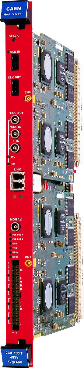

2 Channel 10 bit 4GS/s Digitizer
The Mod. V1761 is the CAEN Waveform Digitizer with the highest sampling rate Flash ADC (10 bit @ 4GS/s).
It can record fast signals from fast organic, inorganic and liquid scintillators coupled to PMTs or Silicon Photomultipliers, Diamond detectors and others, and save them with high efficiency and precision for offline advanced timing analysis. The acquisition can be externally vetoed/gated. Multiple boards can be synchronized to build up complex systems.
The data stream is written in a circular memory buffer with independent read/write access, which reduces the dead-time of the acquisition process.
The acquisition is fully controlled by CAEN WaveDump software, which manages the settings, plots and saves the waveforms. Libraries and demo software in C and LabView are available for integration and customization of specific acquisition systems.
The V1761 comes in a VME form factor with 2 input channels. The communication to and from the board is provided through VMEBus and Optical Link interfaces.
The V1761 fits in the single-slot CAEN VME64X u-crate, which allows you to convert the VME digitizer into a desktop board for lab tests.
Form Factor: 1-unit wide, 6U VME64
Channels: 2 channels single-ended
Bandwidth: 1 GHz
Impedance: 50 Ω
Connector: MCX
Full Scale Range: 1 Vpp
Offset: Programmable DAC for DC offset adjustment in the full-scale range
Resolution: 10 bits
Sampling Rate: 4 GS/s Simultaneously on each channel
Four Altera Cyclone III EP3C16
12-bit/125 MHz DAC FPGA controlled output with four operating modes:
Test pulses: 1 Vpp ramp generator
Majority signal: proportional to the no. of channels under/over the threshold (steps of 125 mV)
Memory Occupancy signal: proportional to the Multi-Event Buffer Occupancy (1 buffer ~ 1mV)
Voltage level: programmable output voltage level
16 general purpose LVDS I/Os controlled by FPGA
Busy, Data Ready, Memory Full, Individual Trg-Out and other functions can be programmed
An Input Pattern from the LVDS I/Os can be associated to each trigger as an event marker
Waveform Recording Firmware: Free firmware for waveform recording
Upgrades: Firmware can be upgraded via Optical Link or VMEBus
Libraries: General purpose C and LabVIEW Libraries
Readout Software: CAEN WaveDump
Configuration Tools: CAEN Toolbox for Firmware upgrade. Direct Register R/W (Example codes)
Compare with Digitizers.
Loading...
| Code | Description |
|---|---|
| WV1761BXAAAA | V1761B - 2 Ch. 10 bit 4 GS/s Digitizer: 7.2MS/ch, EP3C16, DIFF (Obsolete) |
| WV1761CXAAAA | V1761C - 2 Ch. 10 bit 4 GS/s Digitizer: 57.6MS/ch, EP3C16, SE RoHS |
| WV1761XAAAAA | V1761 - 2 Ch. 10 bit 4 GS/s Digitizer: 7.2MS/ch, EP3C16, SE RoHS |
Desktop single-slot VME64X Crate
9U 21Slot VME64X Enhanced Crate series
8U 21 Slot VME64/64X Enhanced Crate Series
7U 21 Slot VME64 Low Cost Crate
7U 21 Slot VME64 Low Cost Crate
2U 4 Slot VME64 Mini Crate
1U 2 Slot VME64 Mini Crate
VME to USB 3.0/Ethernet/Optical Link Bridge
VME to USB 2.0 / Optical Link Bridge
7U CRATE VME/NIM 8 slot VME64 365W, 5 slot NIM 150W
Clock Generator and FAN-OUT
PCI Express Gen 3 CONET2 Controller
USB 3.0 to CONET2 Adapter
Library of functions for CAEN Digitizers high level management
Interface library for CAEN Data Acquistion Modules
Multi-Functional Software Suite for the Upgrade of Front-end Boards, Bridges and Power Supplies
Digitizer Waveform Recording Firmware
+39 0584 388 398
Contacts
What are you looking for?
Search