
Highlights
-
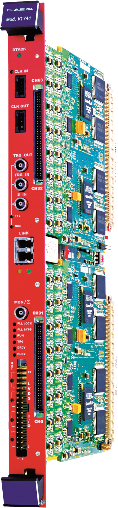
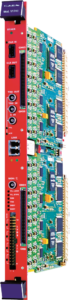
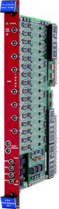
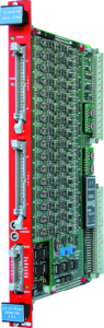
1-unit wide 6U VME64 module
-
1k, 2k, 4k 8k, 16k Peak Sensing ADC
-
64 input channels, single-ended, with 68-pin Dual Row ERNI SMC connector (Zin: 2.5 kΩ)
-
Accepts positive and negative inputs
-
4 Vpp or 8 Vpp Full Scale Range software selectable (3.75 Vpp and 7.5 Vpp when sliding scale is enabled)
-
-
Common Gate mode (64 channels converted at once) with linear gate width or programmable by software
-
Low dead time (about 50 ns after the previous gate closes)
-
Sliding scale algorithm for DNL reduction
-
Zero suppression with programmable threshold
-
Multi-Event Buffer (1024 events)
-
VME64 and Optical link (CAEN CONET proprietary protocol) communication interfaces
-
Windows and Linux drivers, C libraries, demo software
-
Firmware upgradable by the user
Overview
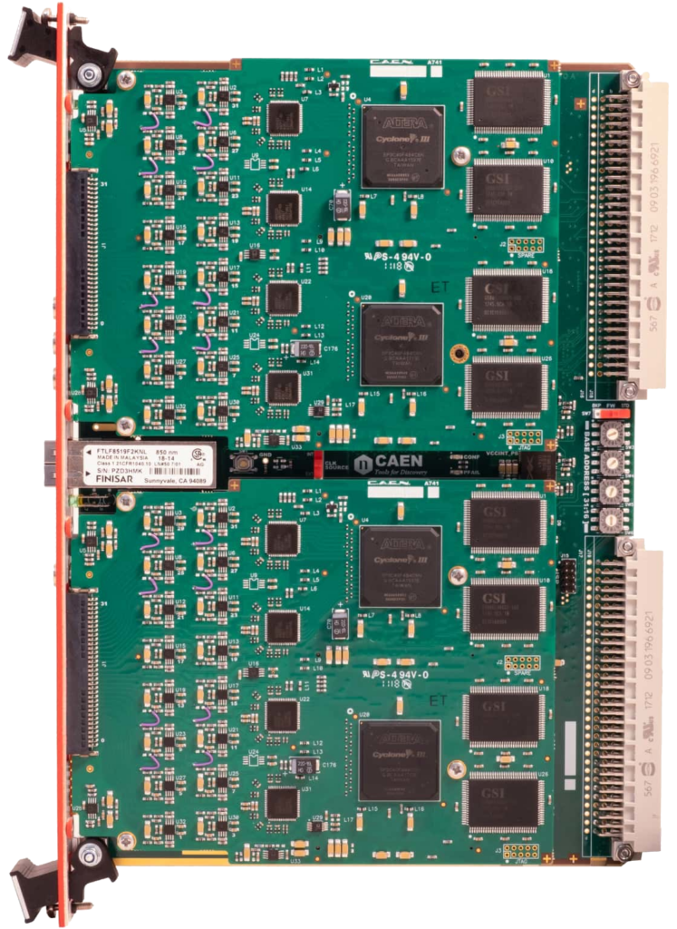
The V1741 is a Digital Peak Sensing ADC belonging to a new generation of detector readout systems based on a mixed analog-digital acquisition chain, combining a high channel density (64 channels) and a low dead time. The FLASH ADC architecture makes it possible to achieve an extremely low conversion time of the pulse peak, so new conversions take place less than 50 ns after the previous gates close.
Conversion gain ranges from 1k up to 16k channels with a low differential non-linearity (DNL) thanks to the sliding scale method.
Receiving the typical slow signal from a Charge Sensitive Preamplifier followed by a Shaping Amplifier (e.g. CAEN N1068), the FPGA identifies the peak of the pulse within a gate by means of digital filters. The acquisition is common to all channels and takes place as soon as the GATE arrives. The energy value together with the time of arrival of the event is first stored in a 1024 multi-event buffer and made available for the readout by VME bus or optical link interface (Daisy-chainable). Both the energy spectrum and the list of events is available through the software interface. Data throughput can be reduced by the Zero Suppression algorithm with a programmable threshold.
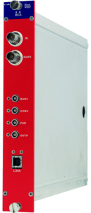
The front panel hosts LEMO (NIM/TTL) inputs that can be used for the GATE, the event discard in case of pile-up (REJ), and the GATE propagation (GPO). The Gate can be linear (same width as the external signal) or re-formed with programmable width.
The V1741 is provided with drivers for the supported communication interfaces, C libraries, demo software for an easy board understanding. Firmware upgrade can be performed via optical link or VMEbus by the user.
Accessories
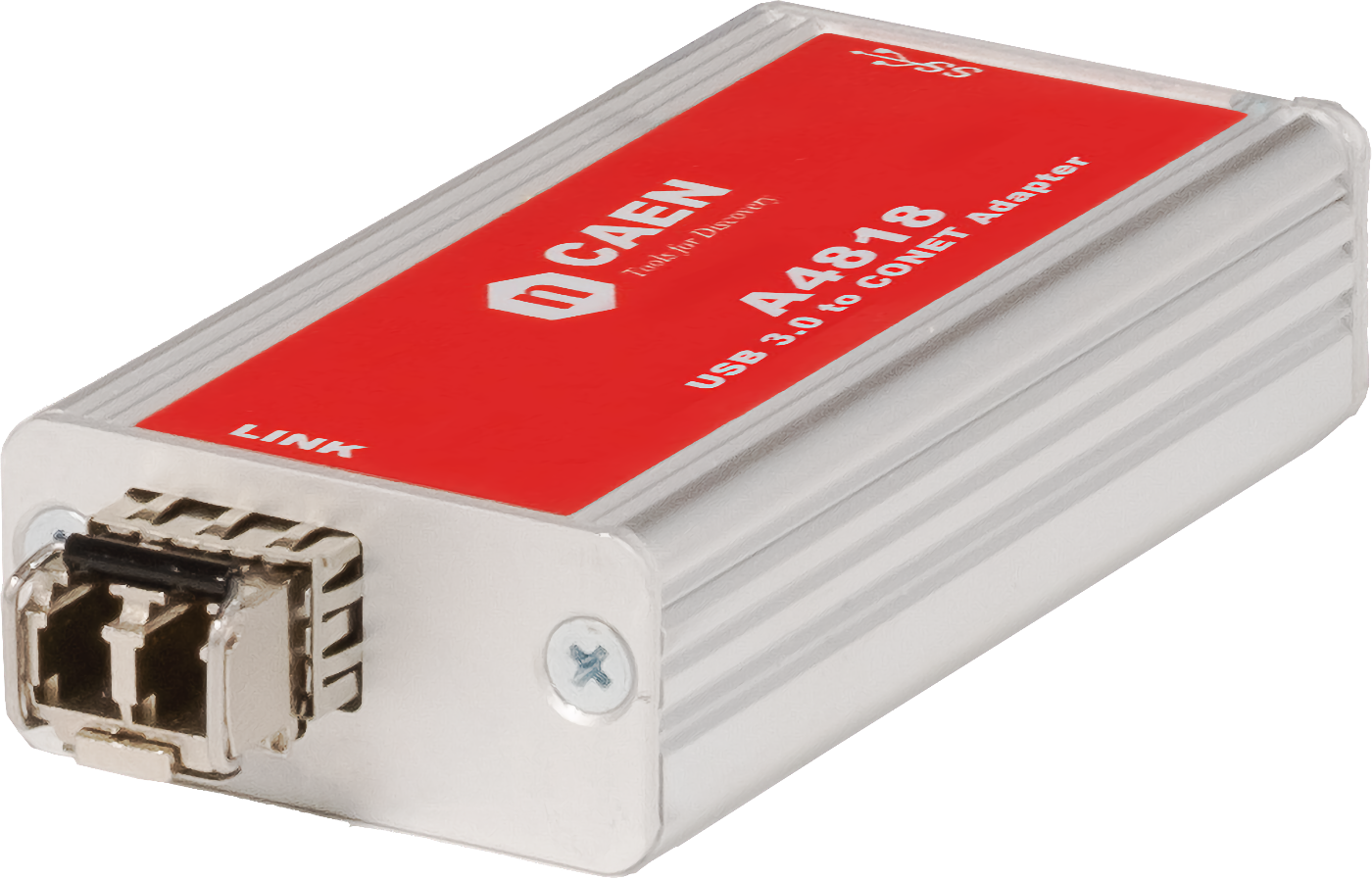
A4818
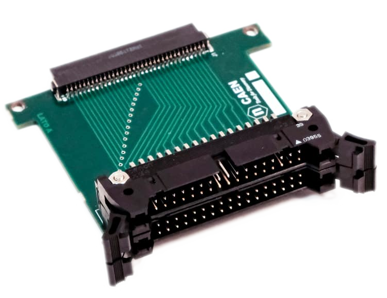
A318
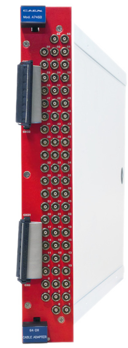
A746B
A317
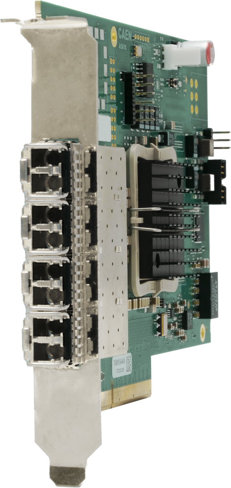
A5818
CONET2 Controller based on PCI Express Gen 3 interface
A371
AI2700
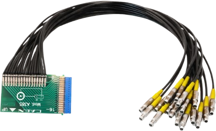
A385
You also may be interested in…
A4818
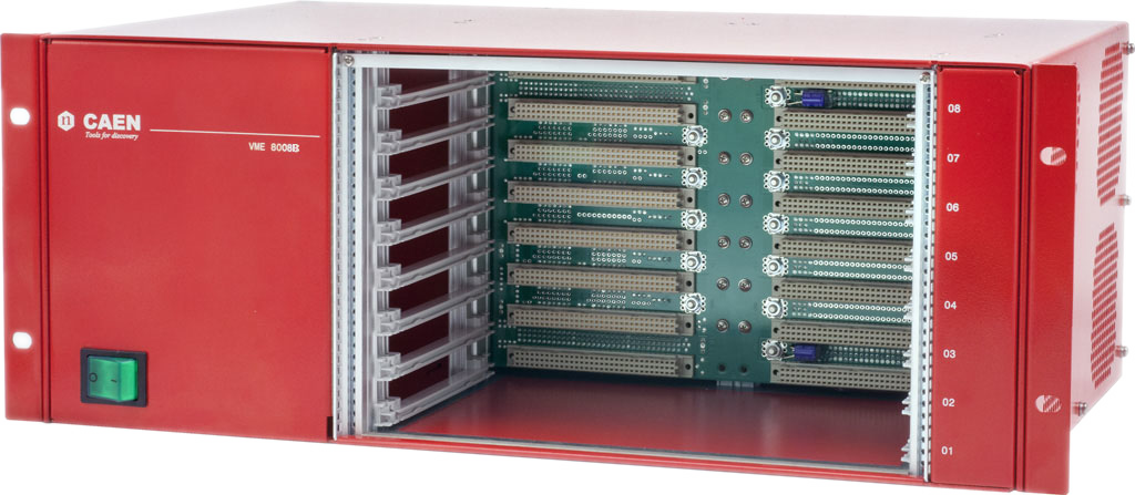
VME8008B

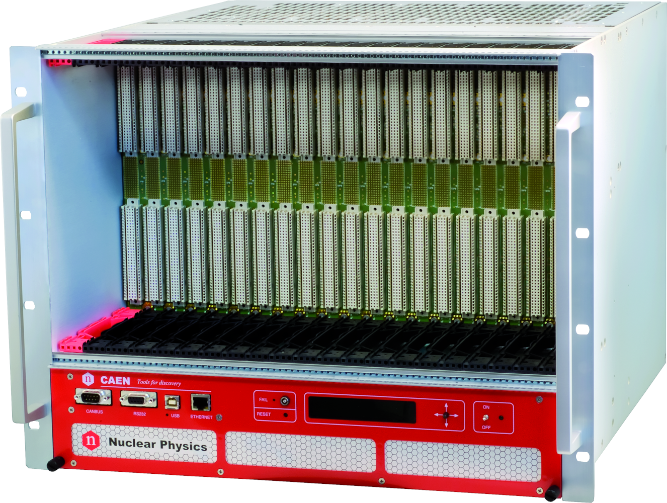
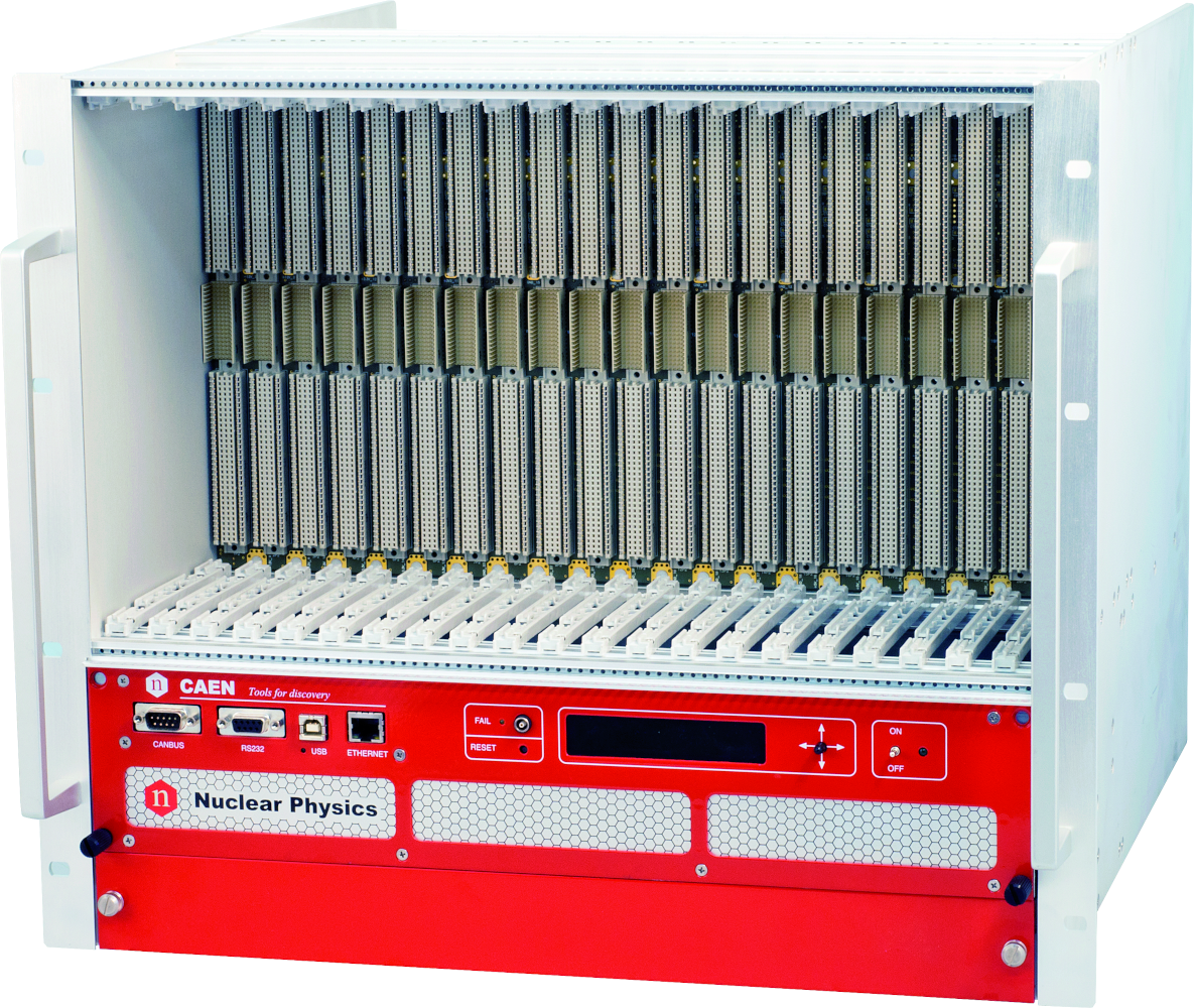
µ-crate
VME8100
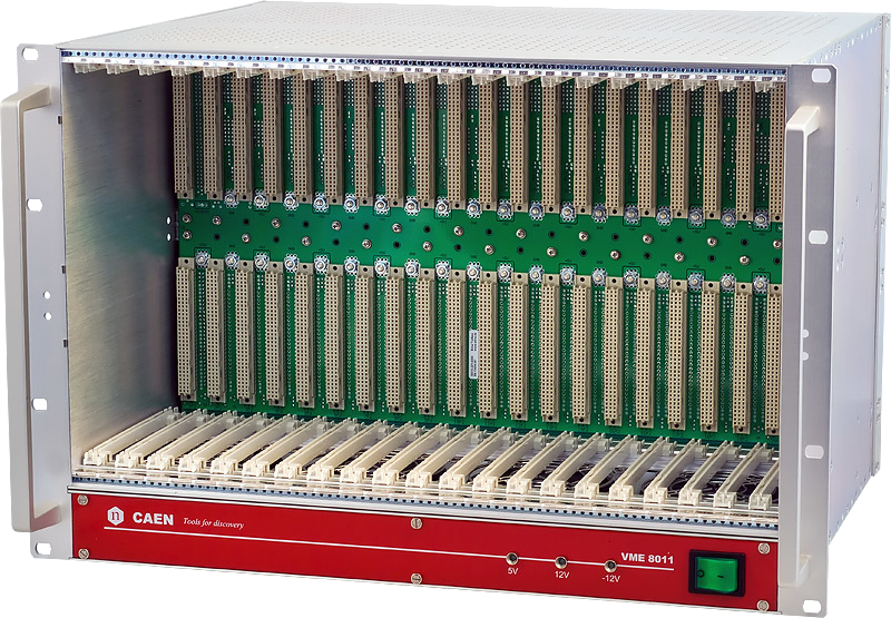
VME8011
VME8200
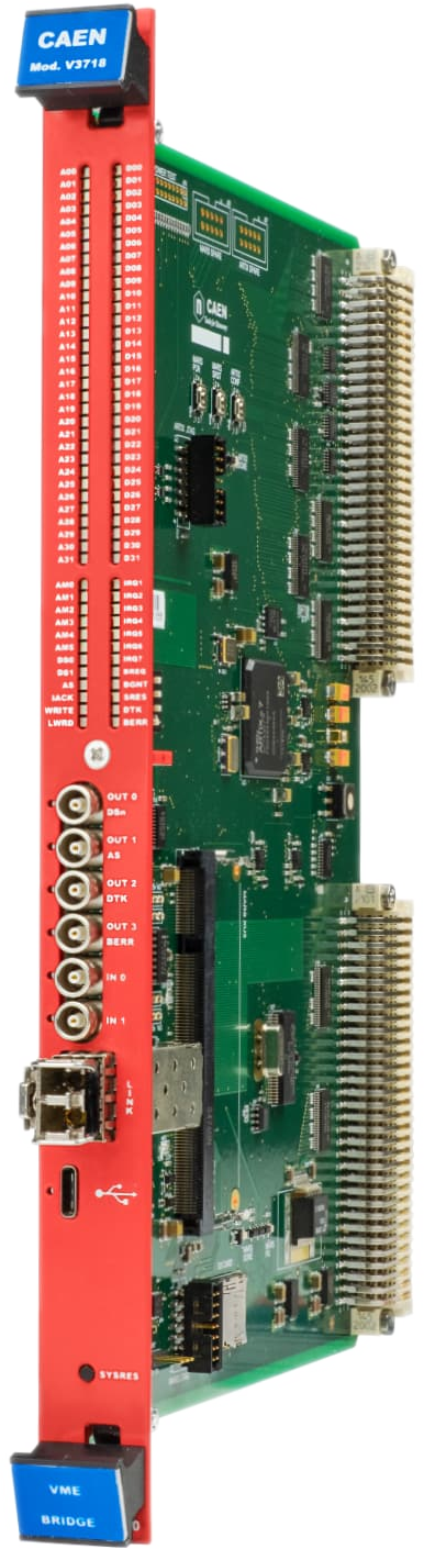
V3718
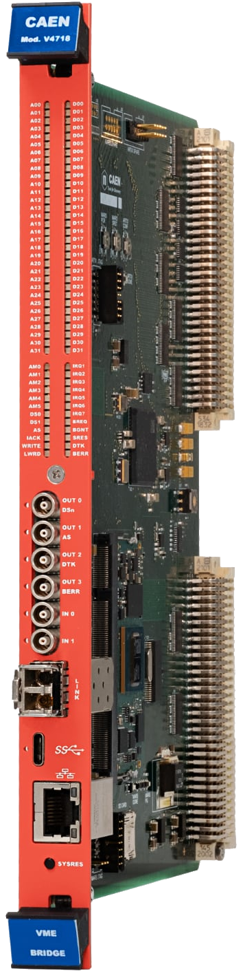
V4718
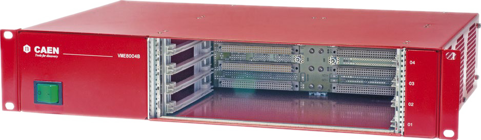
VME8004B
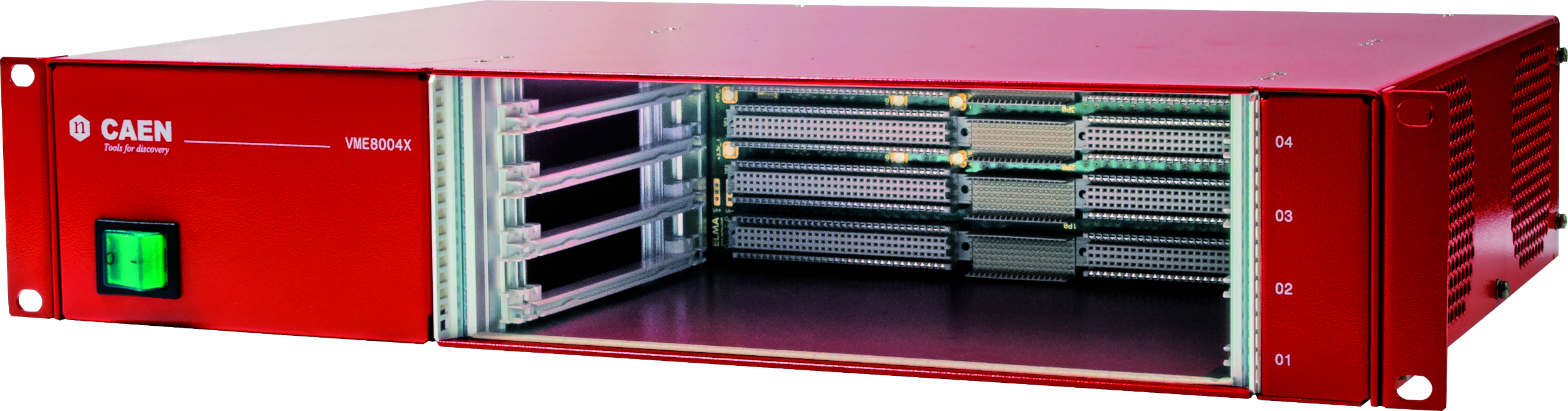
VME8004X
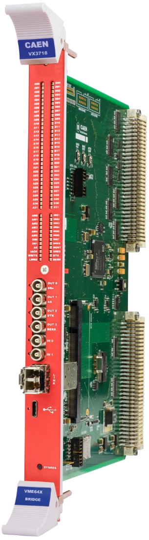
VX3718
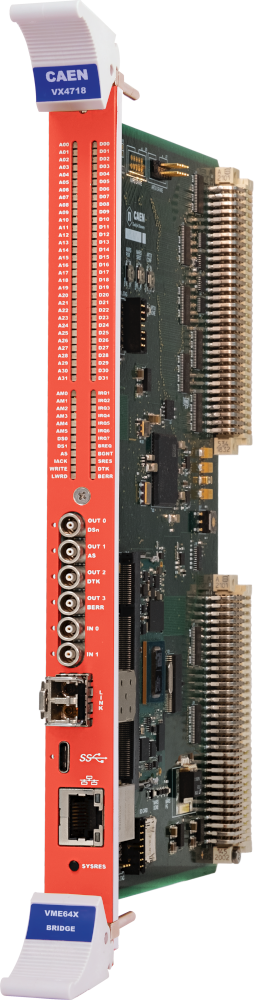
VX4718
VME8008X
Request a Quote

Compare

|
Image
|
Name
|
Package
|
No. of Inputs
|
Resolution (channels)
|
Conversion Time (µs)
|
Full Scale Range (V)
|
Multi Event Buffer size
|
Connectors
|
|
|
V1741 |
VME |
64 |
1k, 2k, 4k, 8k, 16k |
0.1 |
4 |
1024 events / ch |
ERNI SMC |
|
|
N6741 |
NIM |
32 |
1k, 2k, 4k, 8k, 16k |
0.1 |
4 |
1024 events / ch |
ERNI SMC |
|
|
V785N |
VME |
16 |
4k |
2.8 |
4 |
32 events / ch |
LEMO |
|
|
V1785 |
VME |
8 |
4k |
2.8 |
4 / 0.5 (Dual) |
32 events / ch |
LEMO |
|
|
V785 |
VME |
32 |
4k |
5.7 |
4/8 |
32 events / ch |
Std. Flat |
|
|
N957 |
NIM |
1 |
8k |
0.8 |
10 |
64k events / ch |
LEMO |
Technical Specifications
|
GENERAL |
Form Factor: 1-unit wide, 6U VME64 module |
|||
|
ANALOG INPUT |
Channels: 64 channels, Single-ended
|
|||
|
DIGITAL CONVERSION |
Resolution: 12 bits |
|||
|
CONVERSION GAIN |
1k, 2k, 4k, 8k, 16k |
|||
|
DEAD TIME |
50 ns |
|||
|
MINIMUM RISE TIME |
2 ns |
|||
|
INTEGRAL NON LINEARITY (INL) |
< 0.05 % in the range of (1:99) % of the FSR |
|||
|
DIFFERENTIAL NON LINEARITY (DNL) |
< 1 % |
|||
|
ZERO SUPPRESSION |
Zero Suppression threshold common to 8-channel groups and programmable in steps of ADC counts over the entire FSR |
|||
|
GATE |
Gate mode with linear gate width or programmable by software. The GATE signal is fed into the GATE LEMO connector. Gate propagation: Gate_IN/Gate_OUT propagation through the GATE/GPO LEMO connectors |
|||
|
MEMORY |
Multi-event Buffer of 1024 events |
|||
|
DIGITAL I/O |
|
|||
|
TIME STAMP |
48-bit counter, 8 ns step, 16 ns resolution, 625 h range |
|||
|
LVDS I/O |
16 general purpose LVDS I/O controlled by the FPGA: Run, Busy, Veto, Trigger and other functions can be programmed |
|||
|
ADC & MEM. CONTROLLER |
Altera Cyclone EP1C16 (one FPGA serves 16 channels) |
|||
|
COMMUNICATION INTERFACE |
|
|||
|
DPP FW SUPPORTED |
Peak Sensing firmware |
|||
|
FIRMWARE UPGRADE |
Firmware can be upgraded via VMEbus/Optical Link |
|||
|
SOFTWARE |
General purpose C libraries, configuration tools, readout software (Windows and Linux support) |
|||
|
POWER CONSUMPTIONS |
5.4 A @ +5 V; 270 mA @ +12 V, -12 V not used |
Footer