

3 Years Warranty
3 Years Warranty
3 Years Warranty

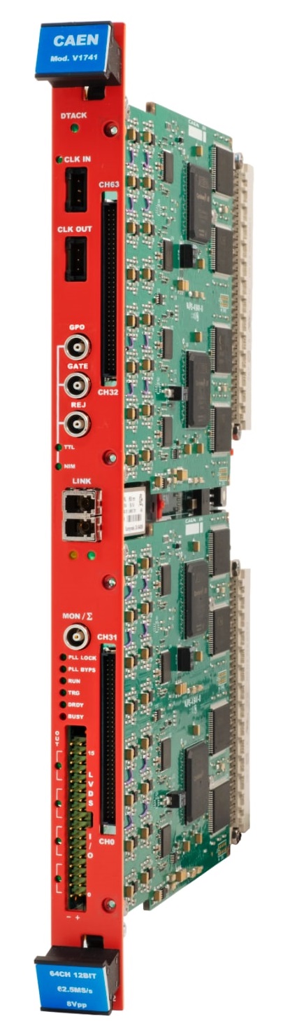
64 Ch Peak Sensing ADC
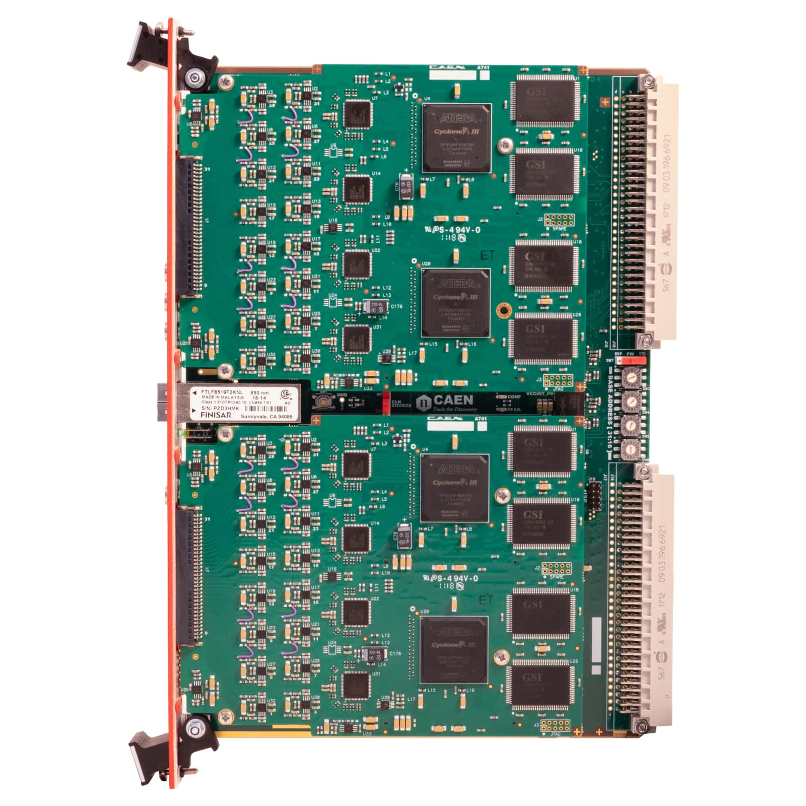
The V1741 is a Digital Peak Sensing ADC belonging to a new generation of detector readout systems based on a mixed analog-digital acquisition chain, combining a high channel density (64 channels) and a low dead time. The FLASH ADC architecture makes it possible to achieve an extremely low conversion time of the pulse peak, so new conversions take place less than 50 ns after the previous gates close.
Conversion gain ranges from 1k up to 16k channels with a low differential non-linearity (DNL) thanks to the sliding scale method.
Receiving the typical slow signal from a Charge Sensitive Preamplifier followed by a Shaping Amplifier (e.g. CAEN N1068), the FPGA identifies the peak of the pulse within a gate by means of digital filters. The acquisition is common to all channels and takes place as soon as the GATE arrives. The energy value together with the time of arrival of the event is first stored in a 1024 multi-event buffer and made available for the readout by VME bus or optical link interface (Daisy-chainable). Both the energy spectrum and the list of events is available through the software interface. Data throughput can be reduced by the Zero Suppression algorithm with a programmable threshold.
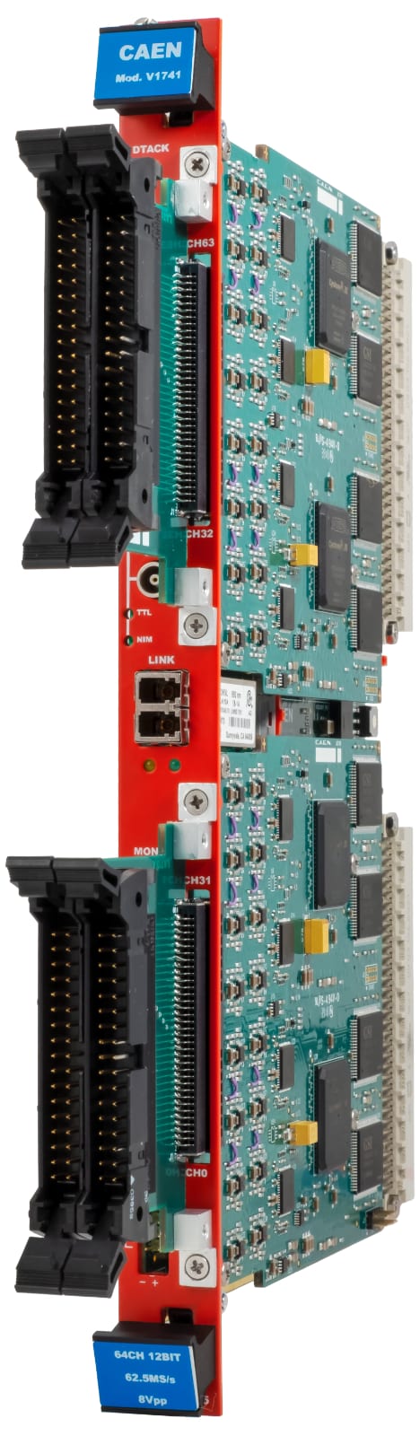
The front panel hosts LEMO (NIM/TTL) inputs that can be used for the GATE, the event discard in case of pile-up (REJ), and the GATE propagation (GPO). The Gate can be linear (same width as the external signal) or re-formed with programmable width.
The V1741 is provided with drivers for the supported communication interfaces, C libraries, demo software for an easy board understanding. Firmware upgrade can be performed via optical link or VMEbus by the user.
Form Factor: 1-unit wide, 6U VME64 module
Weight: 535 g
Channels: 64 channels, Single-ended
Connector: 2 x 68-pin ERNI SMC with 1.27 mm pitch
Impedance: Zin = 2.5 kΩ
Offset: The Sliding Scale automatically manages the DAC for DC offset adjustment on each channel.
Full Scale Range (FSR):
Resolution: 12 bits
Sampling Rate: 62.5 MS/s simultaneously on each channel
1k, 2k, 4k, 8k, 16k
50 ns
2 ns
< 0.05 % in the range of (1:99) % of the FSR
< 1 %
Zero Suppression threshold common to 8-channel groups and programmable in steps of ADC counts over the entire FSR
Gate mode with linear gate width or programmable by software. The GATE signal is fed into the GATE LEMO connector.
Gate propagation: Gate_IN/Gate_OUT propagation through the GATE/GPO LEMO connectors
Multi-event Buffer of 1024 events
CLK-IN (AMP Modu II)
GATE (LEMO)
| CLK-OUT (AMP Modu II)
GPO (LEMO)
| REJ (LEMO)
|
48-bit counter, 8 ns step, 16 ns resolution, 625 h range
16 general purpose LVDS I/O controlled by the FPGA: Run, Busy, Veto, Trigger and other functions can be programmed
An Input Pattern from the LVDS I/O can be associated to each trigger as an event marker
Altera Cyclone EP1C16 (one FPGA serves 16 channels)
| Optical Link | VME
|
Peak Sensing firmware
Firmware can be upgraded via VMEbus/Optical Link
General purpose C libraries, configuration tools, readout software (Windows and Linux support)
5.4 A @ +5 V; 270 mA @ +12 V, -12 V not used
Compare with ADCs (Peak Sensing).
Loading...
| Code | Description |
|---|---|
| WV1741XAAAAA | V1741 64ch Peak Sensing ADC RoHS |
Desktop single-slot VME64X Crate
9U 21Slot VME64X Enhanced Crate series
8U 21 Slot VME64/64X Enhanced Crate Series
7U 21 Slot VME64 Low Cost Crate
7U 21 Slot VME64 Low Cost Crate
4U 8 Slot VME64X Mini Crate
4U 8 Slot VME64 Mini Crate
2U 4 Slot VME64X Mini Crate
2U 4 Slot VME64 Mini Crate
1U 2 Slot VME64 Mini Crate
VME to USB 3.0/Ethernet/Optical Link Bridge
VME to USB 2.0 / Optical Link Bridge
7U CRATE VME/NIM 8 slot VME64 365W, 5 slot NIM 150W
PCI Express Gen 3 CONET2 Controller
USB 3.0 to CONET2 Adapter
+39 0584 388 398
Contacts
What are you looking for?
Search