

3 Years Warranty

16+1 Channel 12 bit 5 GS/s Switched Capacitor Digitizer
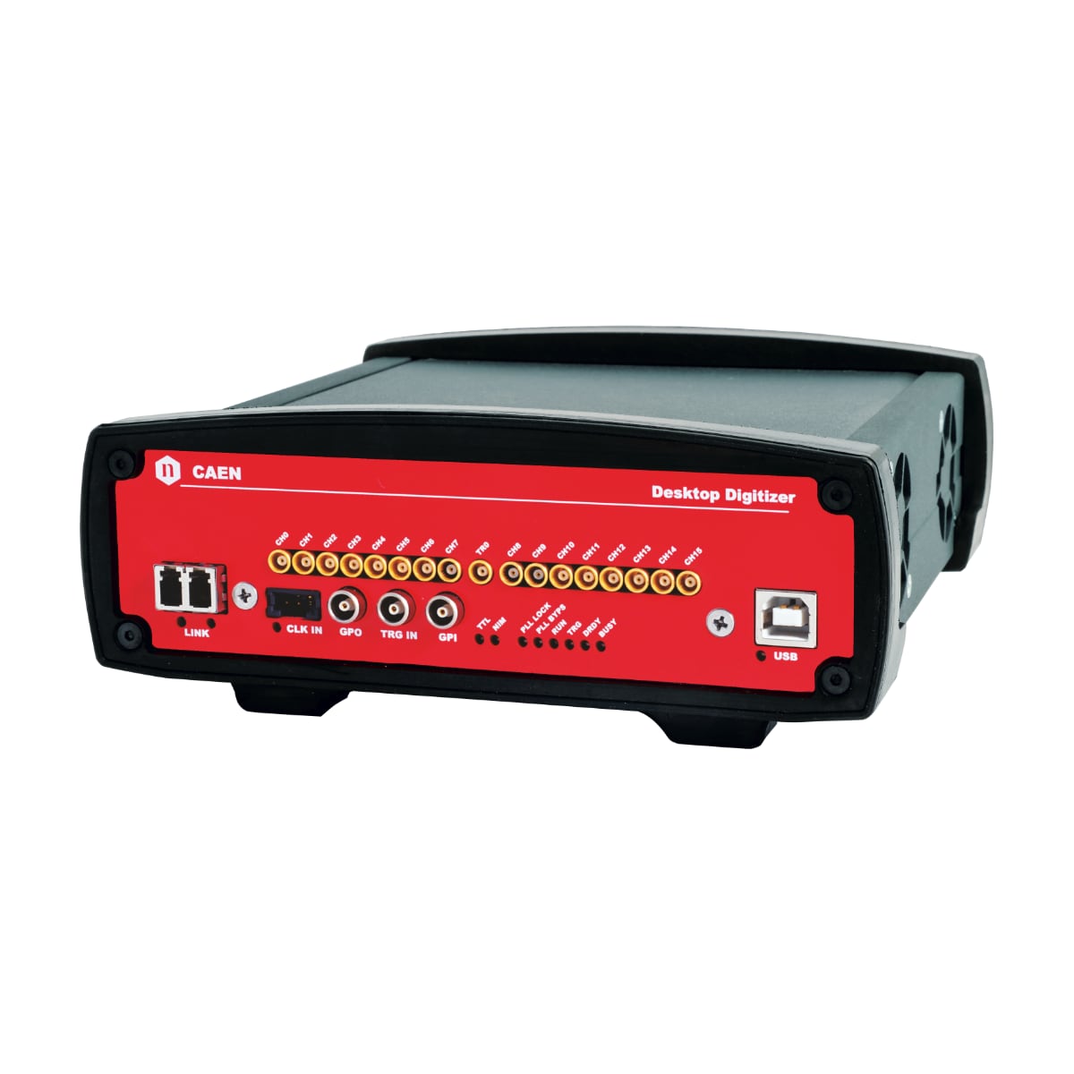
The Mod. DT5742 is a Desktop module housing 16+1 Channel 12 bit 5 GS/s Switched Capacitor Digitizer. The input dynamic range is 1 Vpp on single-ended MCX coaxial connectors (16-bit DAC on each channel to control the DC Offset).
The digitizer is based on the Switched Capacitor Array DRS4 chip (Domino Ring Sampler). This technology relies on a series of 1024 capacitors (analog memory) in which the analog input signal is continuously sampled in a circular way.
The sampling frequency is 5 GHz by default and it can be programmed to 2.5 GHz, 1GHz, and 750 MHz. The analog to digital conversion is not simultaneous with the chip sampling phase, and it starts as soon as the trigger condition is met, thus producing a dead time of 110 μs in case only the analog inputs are digitized, 181 μs when also the fast trigger TR0 is digitized. When the trigger stops the DRS4 chip sampling (holding phase), the analog memory buffer is frozen, and the cell content is made available to the 12 bit ADC for the digital conversion.
The digital memory allows to store subsequent events, even if the readout is not yet started. Moreover, since the digital memory buffers work like FIFOs, the readout activity from USB or Optical Link does not affect write operations of subsequent events.
The available trigger sources are:
The module features the front panel CLK IN connector and an internal PLL for clock synthesis from internal/external references. The module is available with digital memory sizes of 128 event/ch or 1024 event/ch. DT5742 houses USB 2.0 and Optical Link interfaces. USB 2.0 allows data transfers up to 30 MB/s. The Optical Link supports transfer rate of 80 MB/s and offers Daisy chain capability. Therefore, it is possible to connect up to 8/32 ADC modules to a single Optical Link Controller (Mod. A4818/A5818).
Software available (Windows and Linux): CAEN provides drivers for all the different types of physical communication channels, a set of C and LabView libraries (CAENComm and CAENDigitizer), demo applications and utilities:
Software for DT5742 running Waveform Recording Firmware:
Form Factor: Desktop
Weight: 690 g
Dimension: 166 W x 69 H x 171 D mm3
Channels: 16 channels, special channel (TR0) Single ended
Bandwidth: 500 Mhz
Impedance: Zin = 50 Ohm
Absolute max analog input voltage: 3 Vpp (with Vrail max +3V or ‐3V) for any DAC offset
Connector: MCX
Full Scale Range (FSR): 1 Vpp
DC Offset: Programmable 16-bit DAC for DC offset adjustment on each channel. Range ± 1 V
Resolution: 12 bits
Switched Capacitor Array: Domino Ring Sampler chip (DRS4), 8+1 channels with 1024 storage cells each
Sampling Rate: 5 GS/s – 2.5 GS/s – 1 GS/s – 0.75 GS/s SW selectable, simultaneously on each channel
Dead Time (A/D Conversion): 110 μs, analog inputs only. 181 μs, digitizing TR0
Altera Cyclone EP3C16 (one FPGA manages 16+1 channels)
| Trigger Source | Trigger Propagation | Trigger Time Stamp |
|
|
|
| CLK‐IN (AMP Modu II): | GPO (LEMO) | GPI (LEMO) |
| AC coupled differential input clock LVDS, ECL, PECL, LVPECL, CML (single ended NIM/TTL available by A318 adapter) Jitter < 100 ppm requested | Trigger digital output NIM/TTL Zin = 50 Ω TRG‐IN (LEMO) External trigger digital input NIM/TTL Signal Width: > 17 ns Zin = 50 Ω | SYNC/START front panel digital input NIM/TTL Signal Width: > 17 ns Zin = 50 Ω |
Optical Link: CAEN CONET proprietary protocol, Up to 80 MB/s transfer rate, Daisy‐chain capability
USB: USB 2.0 compliant, Up to 30 MB/s transfer rate
Clock Propagation: One‐to‐many: clock distribution from an external clock source to CLK‐IN connector
Acquisition Synchronization: Sync, Start/Stop through digital I/O (GPI or TRG‐IN input / GPO output)
Trigger Time Stamps Alignment: By GPI input connector
Waveform Recording Firmware: Free firmware for waveform recording
Upgrades: Supported via USB/Optical Link
Readout SW: WaveDump readout software with C source files and VS project for developers (Windows® , Linux®)
Libraries and Tools: General purpose C libraries with readout demos (Windows® , Linux® and LabVIEW™ support) and configuration tools
Environment: Indoor use
Operating Temperature: 0◦C to +40◦C
Storage Temperature: –10◦C to +60◦C
Operating Humidity: 10% to 90% RH non condensing
Storage Humidity: 5% to 90% RH non condensing
Altitude: < 2000m
Pollution Degree: 2
Overvoltage Category: II
EMC Environment: Commercial and light industrial
IP Degree: IPX0 Enclosure, not for wet location
EMC: CE 2014/30/EU Electromagnetic Compatibility
Directive Safety: CE 2014/35/EU Low Voltage Directive
1.7 A @ +12 V DC
AC‐DC 12 V/ 45 W power unit included
Compare with Digitizers.
Loading...
| Code | Description |
|---|---|
| WDT5742BXAAA | DT5742B - 16+1Ch. 12 bit 5 GS/s Switched-Capacitor Digitizer: 1024 events/ch (1kS/event), EP3C16,SE RoHS |
| WDT5742XAAAA | DT5742 - 16+1 Ch. 12 bit 5 GS/s Switched-Capacitor Digitizer: 128 events/ch (1kS/event), EP3C16, SE RoHS |
CAEN Digitizer readout application
Library of functions for CAEN Digitizers high level management
Interface library for CAEN Data Acquistion Modules
Multi-Functional Software Suite for the Upgrade of Front-end Boards, Bridges and Power Supplies
Demo Software for x742 Digitizers Synchronization
Digitizer Waveform Recording Firmware
+39 0584 388 398
Contacts
What are you looking for?
Search