Logo Caen

DT5205

Coming Soon

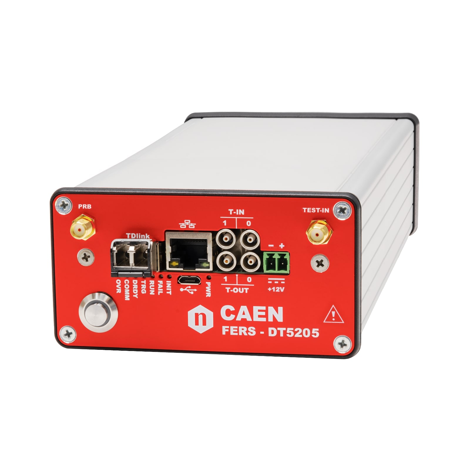
64 Channel Psiroc Desktop unit for FERS-5200

Features

  • 64-channel readout with Weeroc Psiroc ASIC
  • Triggering down to 0.5 fC for sub-20 pF detectors
  • Dual-gain charge measurement and ToT output
  • Sub-ns timing resolution with picoTDC (3.125 ps LSB)
  • Positive/negative input polarity supported
  • Adjustable gain up to 4 V/pC, shaping from 20 ns to 3 μs
  • Low dead time acquisition without multiplexed ADC
  • Fully supported by Janus 5205 software suite
  • Boxed FERS unit (DT5205) for desktop use or unenclosed FERS unit (A5205) for integration into a custom mechanical frame
3 Years Warranty
placeholder
3 Years Warranty
placeholder
3 Years Warranty
placeholder
3 Years Warranty
placeholder
placeholder
placeholder
placeholder
placeholder

Overview

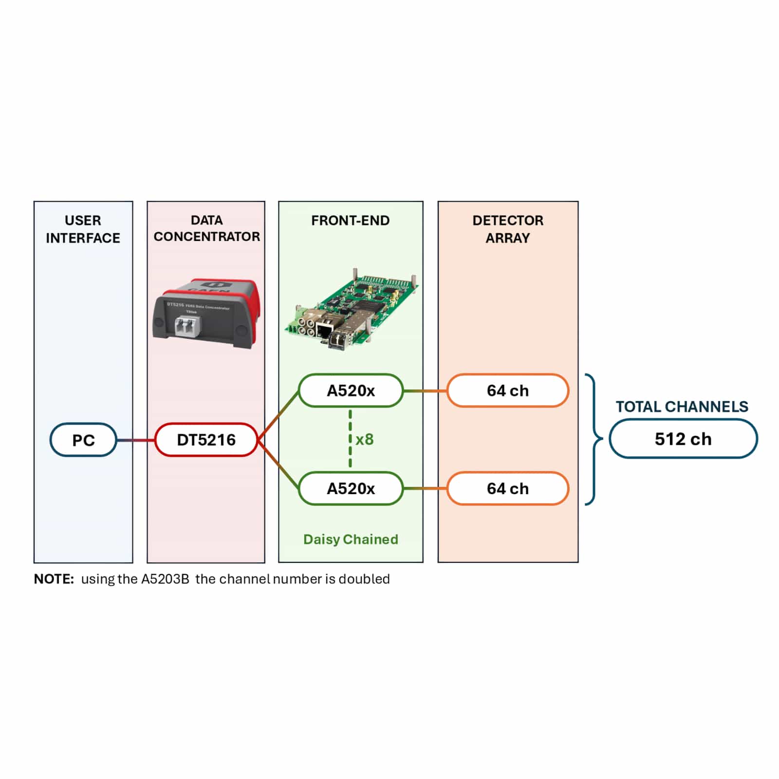
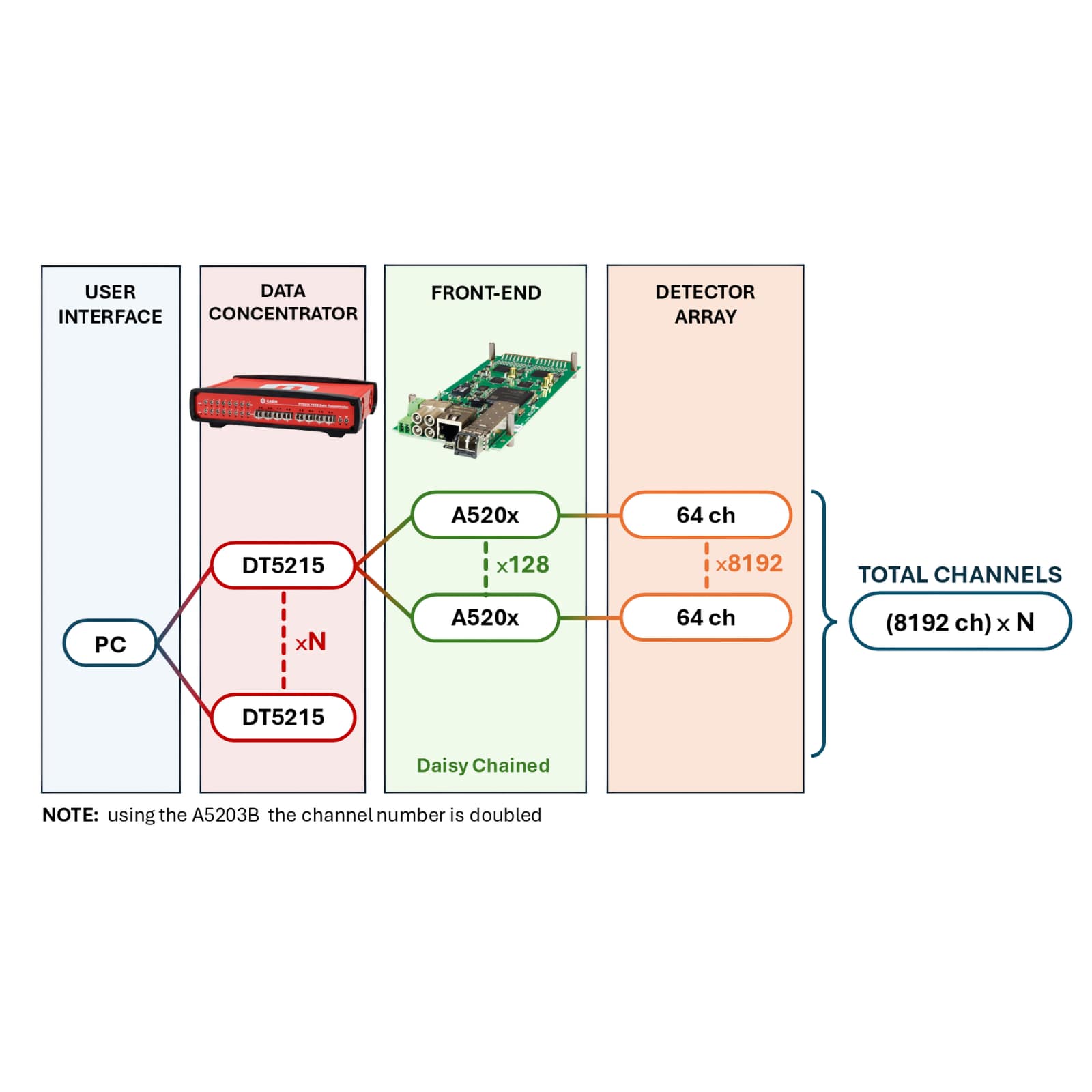
The module DT5205 is a detector readout board suited for PIN diodes, silicon strips and GEMs, handling detector capacitances ranging from 0 up to few hundreds of pF. The module is part of the FERS-5200 family, a Front-End Readout System designed for the readout of large detector arrays such as SiPMs, multi-anode PMTs, Silicon Strip detectors, Wire Chambers, GEM, Gas Tubes and others. FERS is a distributed and scalable system, where each unit is a small card that houses 64 or 128 channels.  It features a detector specific Front-End interfaced to a common infrastructure that guarantees readout interfaces, slow control and synchronization. Typically, the front-end is based on ASIC chips that allow for high density, cost effective integration of multi-channel readout electronics into small size and low power modules. FERS is a flexible platform: combining the same back-end (i.e. readout architecture and interface) with different types of front-end to fit a wide range of detectors.

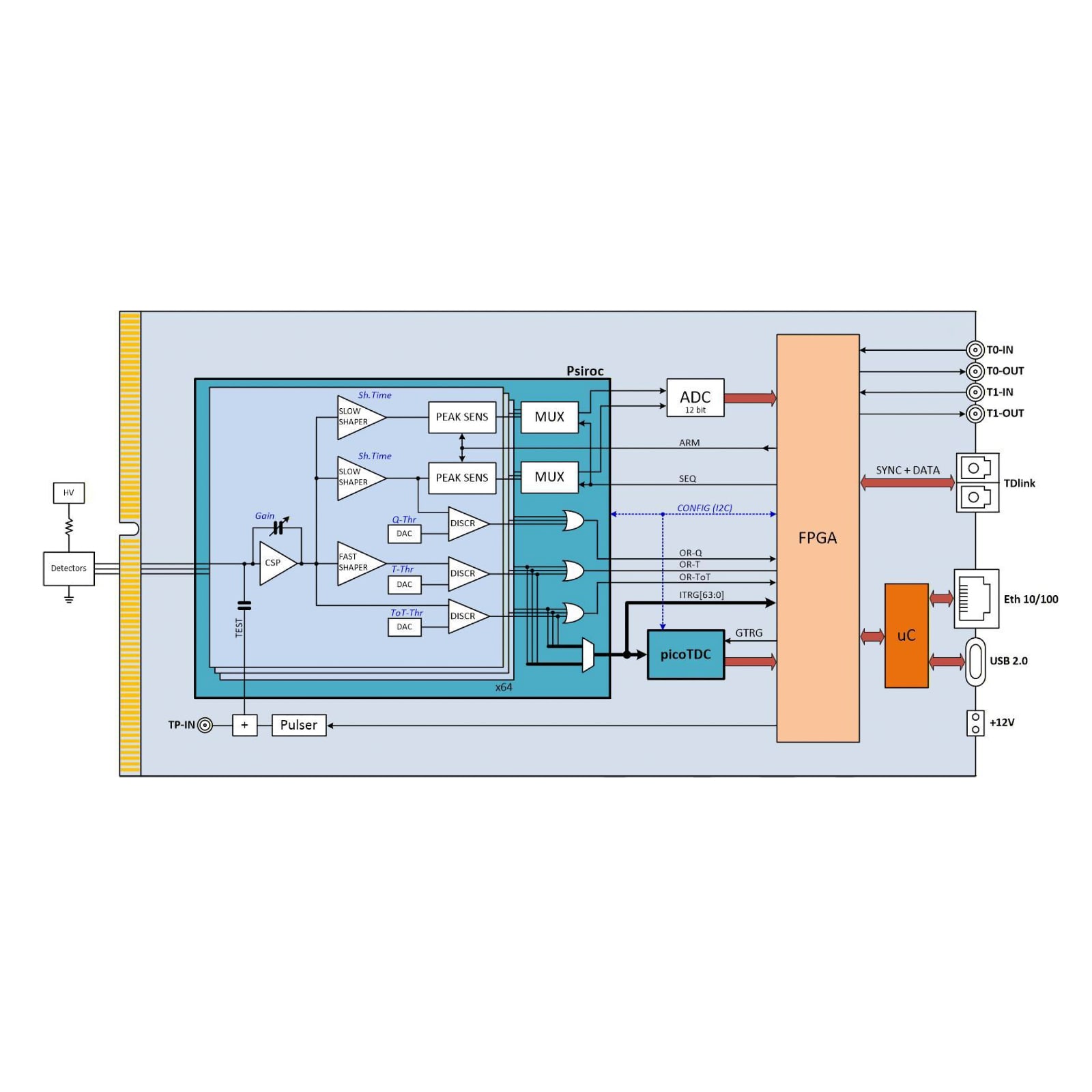
The front end electronics of the DT5205 (and A5205, which is the naked version) is based on the Psiroc chip (produced by Weeroc), that includes a Charge Sensitive Preamplifier (CSP), followed by 2 slow shapers (high and low gain) for the peak sensing ADC and 1 fast shaper for the discriminators that provide triggers and timing information. The individual channel triggers are connected to the FPGA, for hit counting and for triggering, and to a picoTDC, an ASIC chip produced by CERN, implementing a 64 channel TDC with LSB = 12.5 ps, for very precise timing measurements. Time Over Threshold (ToT) can also be used to estimate the pulse height, making it possible to acquire time stamp and PHA with very low dead time and extremely high rate, without the need of the multiplexed A/D conversion.

The most relevant DT5205 acquisition modes are:

  • Spectroscopy Mode: in this mode, the acquisition is simultaneous for the 64 channels of the board. The analog chain made of pre-amplifier (both High and Low gain), shaper and peak sensing is used to acquire the PHA with high energy resolution and wide dynamic range. The common trigger, that initiates the A/D conversion through the multiplexed outputs, can be generated by a combination of the channel self-triggers or from an external signal received from the T0 or T1 inputs. In parallel to the ADC data for the PHA, it is also possible to get high resolution timing information from the picoTDC that receives the individual channel triggers. The event data packet is therefore composed by the common trigger time stamp, trigger ID, dual PHA information (High and Low gains, optionally zero suppressed), individual arrival time of the channel hits that fall in the acquisition window open by the trigger. In spectroscopy mode, after each trigger, there is a dead-time due to the multiplexed A/D conversion. The amount of dead-time is of the order of 30 us, although it depends on the configuration.
  • Counting Mode: the purpose of this acquisition mode is to count the number of self-triggers (i.e. input pulses) of each channel in a time window of programmable size (dwell time). The internal memory buffers allow for saving the channel counts of consecutive time windows, thus implementing a Multi Channel Scaler (MCS) with 64 inputs. The counting mode can also be used to generate the trigger efficiency curves (i.e. counts as a function of the trigger threshold). Looking at these curves, it is possible to define the “zero” of the signal (offset), the minimum threshold above the noise as well as the size of the DAC LSB reported to the input range of the signal.
  • Timing Mode: in timing mode, the peak ADC is disabled and the readout data are only those ones coming from the picoTDC. It is possible to acquire the ToA (Time of Arrival) and/or the ToT (Time over Threshold) of the input pulses. In timing mode, there is no dead-time due to the A/D conversion and there is no need of a common trigger, since the 64 channels are independent and can acquire data in streaming mode, just using their self-triggers (trigger-less acquisition). The ToT can be used to estimate the pulse charge with 1% linearity energy measurement up to 100 pC.
    The timing mode has 2 different options:

    • Trigger Matching: in this mode, there is a trigger signal that defines an acquisition window with arbitrary width and position with respect to the trigger. Only the hits belonging to that window will be recorded. Multiple hits on the same channels will be recorded, as far as there is space in the memory buffers. The acquisition trigger
      can be a combination of the channel self-triggers or an external signal connected to the T0/T1 inputs.
    • Streaming Timing Mode: this acquisition mode implements a continuous hit recording, without any gate or trigger windowing. All hits received by the inputs are time stamped (56 bit) and saved in the form of a sorted list, along with ToT if enabled.


Technical Specifications

GENERAL

Dimensions: 106.1 W x 56.1 H x 186.8 L mm3 (including A5250 pins)
Weight: 503 g

INPUTS

64 channels (= 2 Citiroc-1A chips)

SIGNAL POLARITY

Positive

SENSITIVITY

Dual range: Low Gain (LG)/High Gain (HG). Channel-by-channel individual setting of the gain value through a CSP feedback capacitor, Cf, adjustable from 25 fF to 1575 fF (25 fF step):

  • LG = 1.5 pF/Cf (max gain = 60)
  • HG = 10 x LG = 15 pF/Cf (max gain = 600)
DYNAMIC RANGE

The Citiroc-1A Preamplifiers ensure a dynamic range from 160 fC to 400 pC (i.e. from 1 to 2500 photo-electrons with 106 SiPM gain)

SHAPING TIME

Slow Shaper: 7 options from 12.5 ns to 87.5 ns (12.5 ns step)
Fast Shaper: Fixed 15 ns

FRONT PANEL I/Os

4 general purpose programmable LEMO I/Os connectors available:

  • 2 (T0-IN and T1-IN) to be used as input (LVTTL and NIM)
  • 2 (T0-OUT and T1-OUT) to be used as output (LVTTL)The T1-IN and T0-IN connectors are 50 Ω terminated with a jumper.

The jumper can be moved to perform a bridged connection for daisy chain trigger distribution or wired-OR in a multi-board system.

DIGITAL PROBE

LVTTL signal with different functions can be transmitted via the front panel output connectors.

ANALOG PROBE

SMA connectors allowing the user to acquire analog signals from a specific, software selectable stage of each Citiroc-1A signal shaping chain:

  • LG/HG Preamplifier output
  • LG/HG Slow Shaper output
  • Fast Shaper output
SELF-TRIGGERS
  • Programmable 10-bit DAC for common threshold
  • Minimum threshold: 1/3 photo-electron
  • Separate trigger line per channel
  • Programmable 4-bit DAC for channel-by-channel threshold fine adjustment
  • Logic combination (AND, OR, Majority) of triggers for start of A/D conversion and time reference.
EXTERNAL TRIGGERS

From TDlink, T1-IN or T0-IN. T0/T1 lines can be daisy chained (IN-OUT) or wired-OR (bidirectional) to share a common global trigger between multiple units.

HIGH VOLTAGE POWER SUPPLY

Single channel PCB mounted A7585D High Voltage Power Supply:

  • Common SiPM bias voltage: 20 ÷ 85 V
  • Setting precision: ±0.2%±50 mV
  • Individual channel adjustment: 8-bit (2.5 V or 4.5 V dynamic range, 10% tolerance)
  • Max. output bias current: 10 mA (software programmable limit)
  • Programmable temperature compensation
ACQUISITION MODES

Spectroscopy Mode (PHA)

  • Simultaneous acquisition of all channels
  • 13-bit A/D conversion
  • Systematic conversion time ∼ 10 µs (Max. trigger rate ∼ 100 kHz)
  • Independent digital thresholds for channel-by-channel zero suppression (ZS)

Counting Mode

  • Channel-by-channel independent counting
  • Common trigger to define counting window (Dwell time)
  • Maximum counting rate (per channel):  ∼ 20 Mcps

Timing Mode

  • Independent channels (merged list, time sorted)
  • 0.5 LSB resolution (∼ 250 ps RMS)
  • Time stamp referred to a common time reference coming from T0-IN/T1-IN connectors or from the logic combination of channel self-triggers
  • Spectroscopy information (lower resolution) from Time over Threshold (ToT) information
TIME STAMP
  • 56-bit counter, 8 ns step
  • Up to 128 boards can be synchronized with the DT5215 FERS-CB by sending a time stamp reset signal via TDlink
COMMUNICATION INTERFACES
USB Ethernet Optical Link
  • USB2.0: microUSB connector
  • Bandwidth = ∼ 3 MB/s
  • Ethernet connector, type Rj-45. Supports 10/100 Mbit/s connection to a PC
  • Bandwidth = ∼ 2.5 MB/s
  • Small Form Factor Pluggable (SFP+) transceiver component for optical connection (3.125 Gbit/s). TDlink CAEN proprietary protocol allows for multi-board synchronization, slow control and data
    readout
  • Data Concentrator DT5215 required


FIRMWARE

Firmware can be upgraded via USB, Ethernet or Optical Link (starting from firmware revision 7.5)

SOFTWARE

Readout SW
Fully controlled by the Janus open source software for Windows® and Linux®.
It can run in console mode (C program, with console commands and gnuplot display for plots) or connected to a GUI (Python) that implements user friendly configuration panels and run controls.

Janus can acquire, plot and save output files with PHA, ToT histograms, as well as list files (energy and timestamp for each channel).

Web Interface
Board information and monitoring, Ethernet configuration.

POWER REQUIREMENTS

Single power supply (+12 V). Regularly working in a range between +7 V and +15 V

POWER CONSUMPTIONS

750 mA @ +12 V, i.e. ≈ 9 W (acquisition on, all channels enabled, HV on, 64 SiPMs mounted)
685 mA @ +12 V, i.e. ≈ 8.2 W (acquisition off, all channels enabled, HV off, no SiPMs mounted)

Compare

Compare with FERS-system.

Loading...

Accessories

A5253
3-pin header adapter for A5202/DT5202 & A5204/DT5204
A5260
Remotization cable for FERS-5200 boards
A5250
2.54 mm pin header adapter for A5202/DT5202 & A5204/DT5204

Ordering Options

Code Description
WDT5205XAAAA DT5205 - 64 channel Psiroc unit for FERS-5200 with picoTDC   RoHS

Contacts

Great to have you back!

Sign In with Auth CAEN