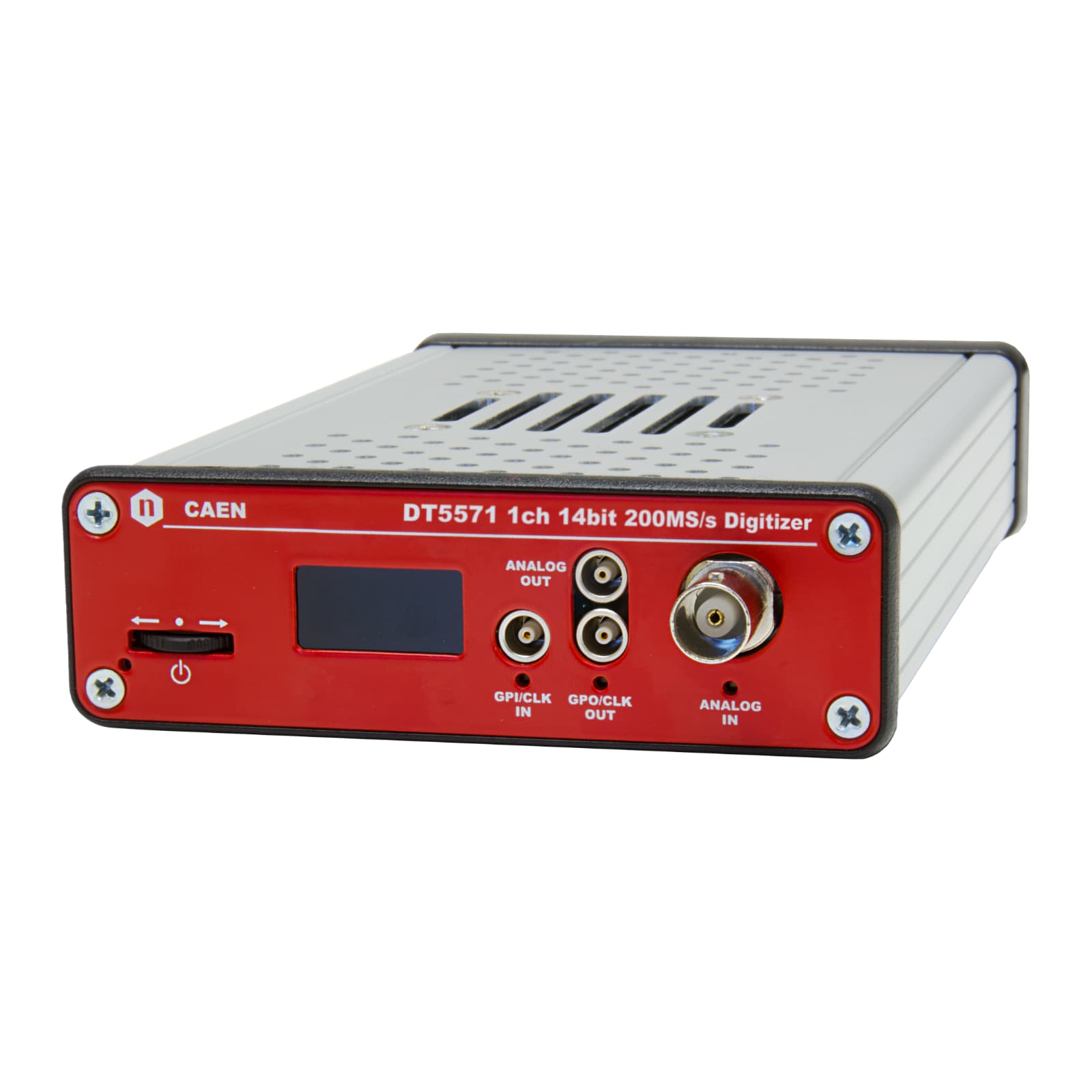
Logo Caen

DT5571

Coming Soon

1 Channel 14-bit 200 MS/s Open FPGA Digitizer

Features

  • 1 analog input, 14-bit @ 200 MS/s, 50 Ω
  • Scope & DPP modes with internal memory buffer
  • Open FPGA – user firmware via Sci-Compiler
  • USB 2.0 and 10/100 Mb Ethernet interfaces
  • Compatible with WaveDump and CoMPASS
  • Available as desktop version

Overview

The DT5571 is a high-performance waveform digitizer featuring 14-bit resolution and a 200 MS/s sampling rate on a single analog input. Designed to meet the needs of modern acquisition setups, it combines precision, speed, and flexibility in a streamlined desktop form factor.
Two operating modes are supported: Scope Mode for raw waveform recording, and DPP Mode for real-time on-board signal processing. With software-selectable input polarity and an internal memory buffer, the DT5571 is ideal for reading out scintillators, SiPMs, and other fast detectors.
The module offers USB 2.0 and 10/100 Mb Ethernet interfaces for fast data transfer and remote access. Its Open FPGA architecture enables full customization of acquisition logic via CAEN’s Sci-Compiler, with a graphical environment accessible to users with no VHDL experience.
It is also fully compatible with WaveDump2 and CoMPASS, supporting both advanced analysis and straightforward configuration. Whether for R&D, prototyping, or education, the DT5571 delivers reliable performance and flexibility in a compact, lab-friendly solution.
The DT5571 is available in desktop version and is ready to support your next acquisition challenge.
In collaboration with Nuclear Instruments.

Technical Specifications

GENERAL

Form Factor: Desktop 257 x 102 x 331 mm3 (WxHxD)

ANALOG INPUT

Channels: 1 BNC type
Impedance: 50 Ω/1 kΩ programmable
Bandwidth: 60 MHz, Programmable DC offset adjustment on each input in the full scale range
Analog Coarse Gain: [x1:x100]
Full Scale Range: [0.015 Vpp: 1.5 Vpp]

DIGITAL I/Os

USER IO 0…2 (LEMO)

  • Programmable Digital I/Os, function stated at firmware level.
  • Can be used as Trigger, Start, Busy
  • Single-ended, Zin / Rt = 50 Ω
DIGITAL CONVERSION

Resolution: 14 bits
Sampling Rate: 200 MS/s

CLOCK GENERATION

200 MHz ADC clock

Clock sources: internal/external

  • Internal 25 MHz oscillator
  • External 25 MHz – USER IN 0 or SYNC connector
TRIGGER
Trigger Propagation 

  • Through USER I/Os and Sync Connector
Trigger Source 

  • Internal/External: managed by the default firmware
  • Complex trigger logic: implementable by the user on the open FPGA
Trigger Time Stamp 

  • Default FW: 32-bit counter, 8 ns resolution, 26-day range
  • Custom FW: defined by the firmware design
SYNCHRONIZATION

Clock Propagation: USER I/Os connectors SYNC Connector

Acquisition Synchronization

  • Through programmable LEMO
  • Through dedicated SYNC Connector

Sync connector allows to cascade multiple units and synchronize them with a single standard CAT5e cable

FPGA

Open FPGA: Xilinx Zynq-7000 SoC Z-7030

MEMORY
  • 1 GByte of memory for list readout on each SoC
  • Up to 8kS/ch for simultaneous waveform readout
COMMUNICATION INTERFACE

The different readout interface allows to integrate the DT5560SE in existing experimental environment.

Ethernet 

1 Gbps

USB2.0 

1x mini-USB

Optical Link 

  • Slots for 2 x 10 Gbps SFP + transceivers
  • (communication protocol not implemented by default)
FIRMWARE

Default

  • Waveform recording and Pulse Height Analysis
  • Ethernet/USB communcation

Custom

  • Use Sci-Compiler to develop your own firmware
FIRMWARE UPGRADE

Firmware can be upgraded via Ethernet, mini-USB or JTAG mini-USB debugger (on-the-fly)

SOFTWARE
  • SCI-55X0 Readout Software to manage the default firmware
  • Sci-Compiler for custom firmware development
POWER REQUIREMENTS
  • Voltage: 100-240 Vac
  • Frequency: 50/60 Hz
  • Typ. power consumption: 300 mA @ 220 Vac

Compare

Compare with Digitizers.

Loading...

Contacts

Great to have you back!