

3 Years Warranty

8 Channel 12bit 3.2 GS/s Switched Capacitor Digitizer
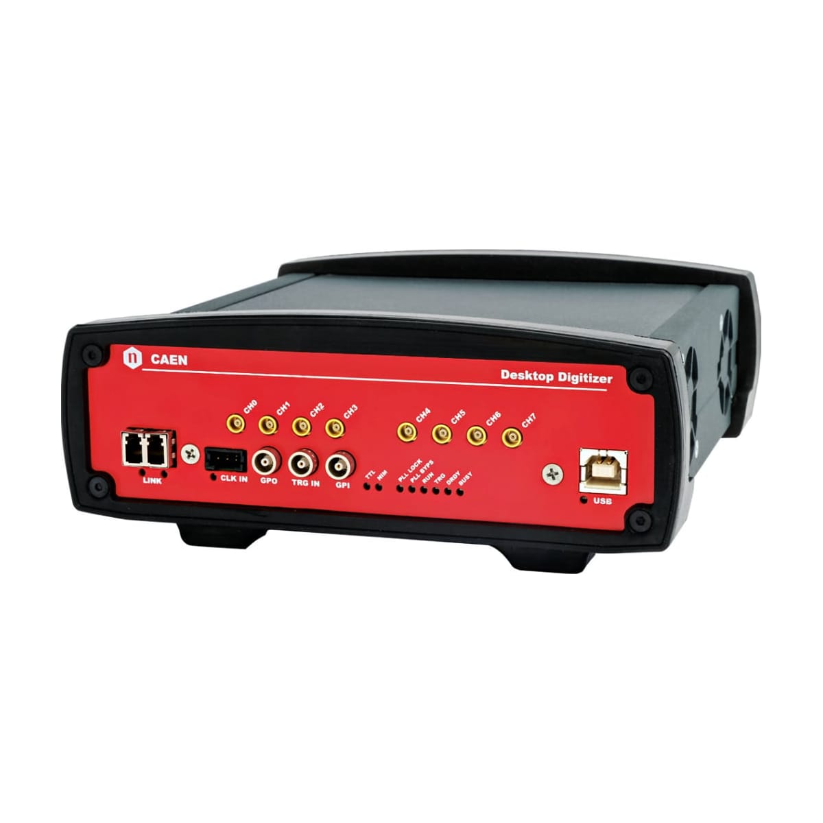
The Mod. DT5743 is a Desktop module housing 8 Channel 12 bit 3.2 GS/s Switched Capacitor Digitizer, with 2.5 Vpp single-ended input dynamics, issued from the collaboration with CEA/IRFU & CNRS/IN2P3/LAL and based on SAMLONG chip. A programmable DAC on each channel allows for DC Offset adjustment in the ±1.25 V range.
The analog input signals are continuously sampled into the SAMLONGs (sampling intervals down to 312.5 ps) in a circular analog memory buffer (1024 cells). As a trigger signal arrives, all analog memory buffers are frozen and subsequently digitized with a resolution of 12 bits into a digital memory buffer. During analog to digital conversion process, the DT5743 cannot handle other triggers (Dead Time: 125 us).
The memory buffer allows to store up to 7 full events for each cannel (1 event = 1024x12bit). The buffer can be read by USB or Optical Link simultaneously with write operation of successive events.
The module features front panel Clock Input and a PLL for clock synthesis from internal/external references. DT5743 supports multi-board synchronization allowing all switched capacitor memories to be synchronized to a common clock source and ensuring Trigger time stamps alignment. Once synchronized, all data will be aligned and coherent across multiple DT5743 boards
Each channel is equipped with an individual discriminator, with programmable threshold, which generates a trigger request when the input signal goes over threshold. The trigger requests from the channels are processed by the board to generate a common trigger causing all the channels to acquire an event simultaneously. The common trigger can also be provided externally via the front panel Trigger Input or via the software, for debug purposes, through VMEbus/Optical Link.
DT5743 houses USB 2.0 and Optical Link interfaces. USB 2.0 allows data transfers up to 30 MB/s. The Optical Link supports transfer rate of 80 MB/s and offers Daisy chain capability. Therefore, it is possible to connect up to 8/32 ADC modules to a single Optical Link controller (Mod. A4818/A5818).
Mod. DT5743 features an embedded Charge Mode, where the pulse integration window is defined by the user (high rates ~3.5 KEvents/s). This feature allows to perform on-line processing on detector signal directly digitized.
Some typical applications:
Software available (Windows and Linux):
CAEN provides drivers for all the different types of physical communication channels, a set of C libraries (CAENComm and CAENDigitizer) for Windows and Linux OS, as well as a control software tool for Windows:
Form Factor: Desktop
Weight: 680 g
Dimension: 166 x 69 x 171 mm3 (WxHxD)
Channels: 8 channels single ended
Bandwidth: 500 MHz
Impedance: 50 Ω
Absolute max analog input voltage: ± 3.5 V
Connector: MCX
Full Scale Range: 2.5 Vpp DC coupled
Offset: Programmable 16-bit DAC for DC offset adjustment on each channel. Range: ± 1.25 V
One pulser per channel with programmable 16-bit pattern (fixed amplitude)
| Analog Memory (Switched Capacitor Array)
SAMLONG Fast Analog Memory chip |
Resolution
12 bits Sampling Rate 3.2/1.6 /0.8/0.4 GS/s |
Dead Time (Event A/D Conversion)
125 µs (max. @ 1024 samples) decreasing proportionally with the recording depth (configurable record length) |
Altera Cyclone EP3C16 (one FPGA manages 4 channels)
| Trigger Source
– Self-trigger: channel over/under threshold (based on analog discriminator on each channel with DAC adjusted threshold) for Common trigger generation – External-trigger: Common by TRG-IN connector (NIM/TTL, LEMO, Zin = 50 Ω) – Software-trigger: Common by software command |
Trigger Propagation
GPO programmable digital output (NIM/TTL, |
Trigger Threshold
Programmable thru a 16-bit DAC in the ±1.25 V range on each channel |
Trigger Time Stamp
40-bit counter, 5 ns resolution, 83 minutes range |
< 8 ps RMS (5 ps RMS typical) @ 3.2GS/s obtained at thermal regime, after INL time calibration and with dual-pulse timing measurement by pulse generator.
Test conditions: periodic input pulses with 1V Amplitude, 1kHz Frequency, rise time of 0.8/1.6/2.5 ns; the resolution does not change significantly when varying the delay Δt between the two pulses.
Note: it is recommended to provide proper cooling to improve the resolution performances
Sampling Time Precision
< 20 ps @ 3.2 GS/s (before calibration)
< 5 ps @ 3.2 GS/s (after calibration)
Note: obtained with factory calibration and dual-pulse timing measurement with pulse generator.
Test conditions:
The resolution does not change significantly when varying the delay Δt between the two pulses.
Noise Level: 0.75 mV RMS
CLK-IN (AMP Modu II)
|
TRG-IN (LEMO)
External trigger or Start/Stop acquisition digital input: NIM/TTL, Zin = 50 Ω |
GPI (LEMO)
Trigger Time Stamp reset or Start/stop acquisition digital input: NIM/TTL, Zin = 50 Ω |
GPO (LEMO)
Common trigger digital output: NIM/TTL, Rt = 50 Ω |
Clock Propagation
One-to-many clock distribution from an external clock source, typically at 50 MHz, on CLK-IN (AC coupled differential input clock: LVDS, ECL, PECL, LVPECL, CML on AMP MODU II connector)
Clock Cable delay compensation
Acquisition Synchronization
Trigger Time Stamps Alignment
By GPI input connector
Altera Cyclone EP3C16 (1 FPGA serves 4 channels)
Optical Link: CAEN CONET proprietary protocol, up to 80 MB/s transfer rate Daisy chainable: it is possible to connect up to 8/32 ADC modules to a single Optical Link Controller (Mod. A4818/A5818)
USB: USB 2.0 compliant Up to 30 MB/s transfer rate
Software selectable embedded Charge Mode for input pulse high rate charge integration and fast histogramming
Normal Mode (default): Waveform recording
Charge Mode (sw selectable): Input pulse high-rate charge integration
Upgrades: Supported via USB/Optical Link
Environment: Indoor use
Operating Temperature: 0◦C to +40◦C
Storage Temperature: –10◦C to +60◦C
Operating Humidity: 10% to 90% RH non condensing
Storage Humidity: 5% to 90% RH non condensing
Altitude: < 2000m
Pollution Degree: 2
Overvoltage Category: II
EMC Environment: Commercial and light industrial
IP Degree: IPX0 Enclosure, not for wet location
EMC: CE 2014/30/EU Electromagnetic Compatibility Directive
Safety: CE 2014/35/EU Low Voltage Directive
Compare with Digitizers.
Loading...
| Code | Description |
|---|---|
| WDT5743XAAAA | DT5743 - 8 Ch. 12 bit 3.2GS/s Switched-Capacitor Digitizer: 7 events/ch (1kS/event), EP3C16, SE RoHS |
CAEN x743 Digitizer Readout Application
Oscilloscope Tool for 743 digitizer family
Library of functions for CAEN Digitizers high level management
Interface library for CAEN Data Acquistion Modules
Multi-Functional Software Suite for the Upgrade of Front-end Boards, Bridges and Power Supplies
Digitizer Waveform Recording Firmware
+39 0584 388 398
Contacts
What are you looking for?
Search