

3 Years Warranty
3 Years Warranty
3 Years Warranty
3 Years Warranty

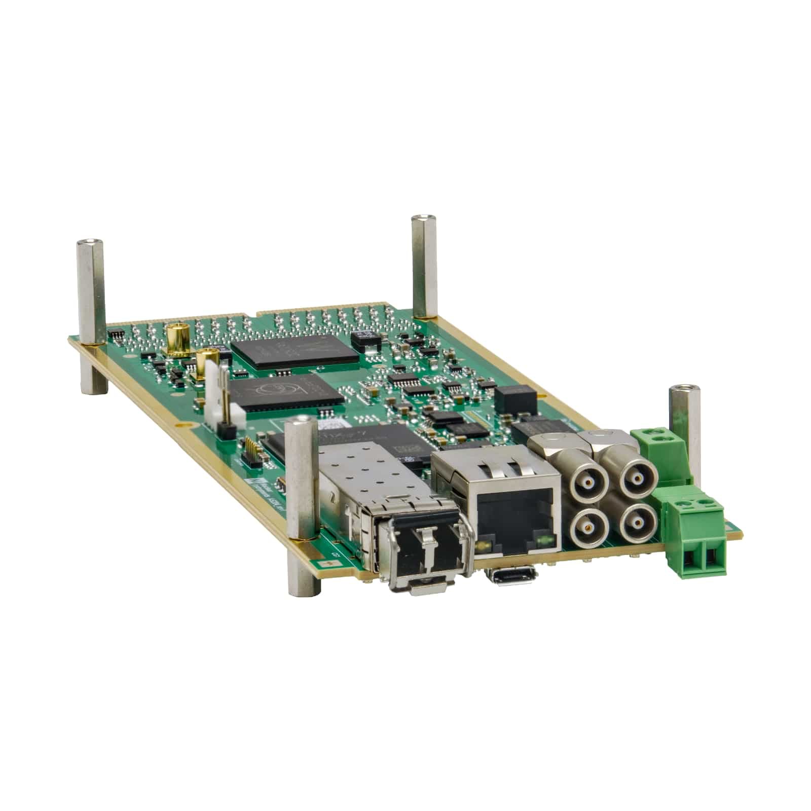
64 Channel Psiroc unit for FERS-5200
The module A5205 is a detector readout board suited for PIN diodes, silicon strips and GEMs, handling detector capacitances ranging from 0 up to few hundreds of pF. The module is part of the FERS-5200 family, a Front-End Readout System designed for the readout of large detector arrays such as SiPMs, multi-anode PMTs, Silicon Strip detectors, Wire Chambers, GEM, Gas Tubes and others. FERS is a distributed and scalable system, where each unit is a small card that houses 64 or 128 channels. It features a detector specific Front-End interfaced to a common infrastructure that guarantees readout interfaces, slow control and synchronization. Typically, the front-end is based on ASIC chips that allow for high density, cost effective integration of multi-channel readout electronics into small size and low power modules. FERS is a flexible platform: combining the same back-end (i.e. readout architecture and interface) with different types of front-end to fit a wide range of detectors.
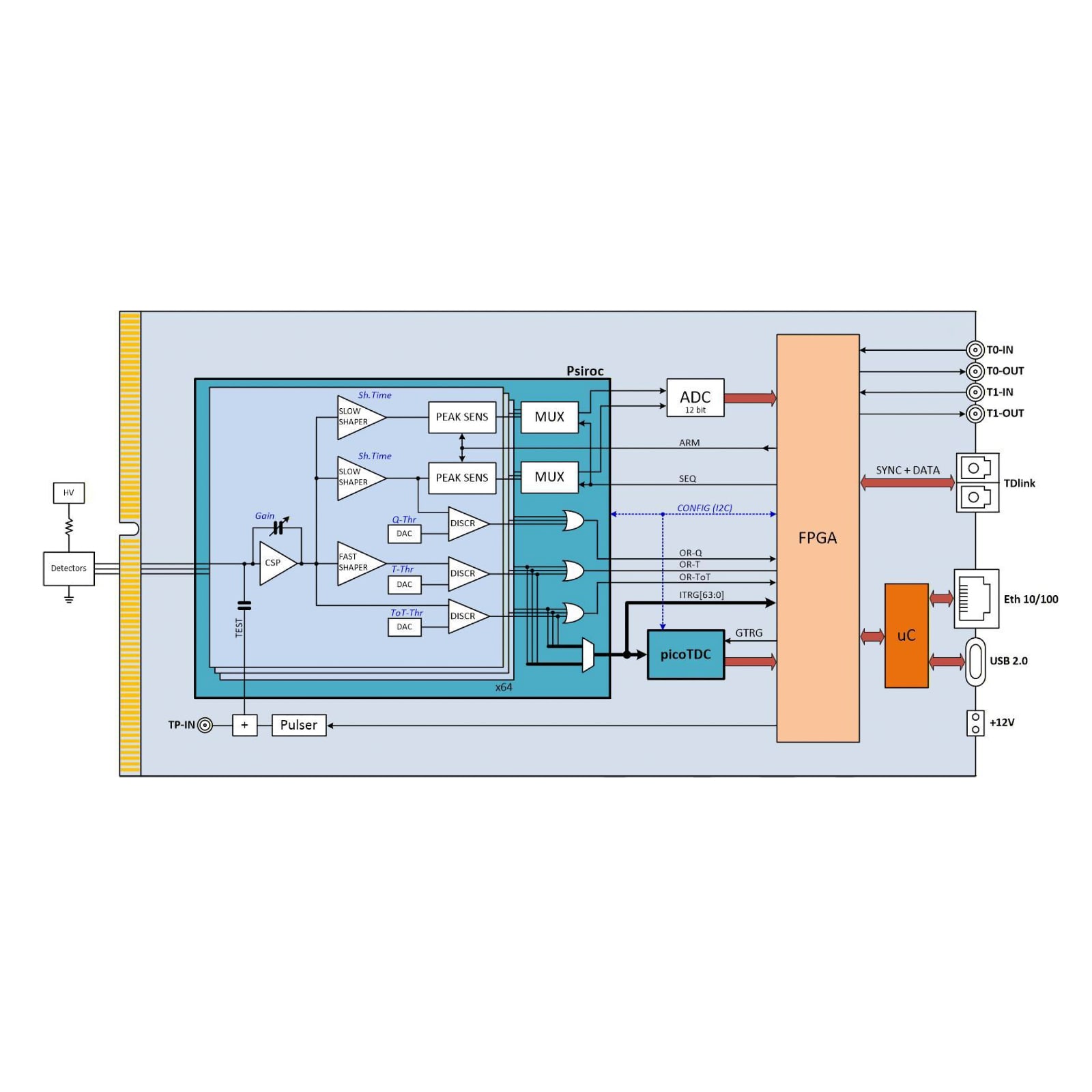
The front end electronics of the A5205 (and DT5205, which is the boxed version for desktop use) is based on the Psiroc chip (produced by Weeroc), that includes a Charge Sensitive Preamplifier (CSP), followed by 2 slow shapers (high and low gain) for the peak sensing ADC and 1 fast shaper for the discriminators that provide triggers and timing information. The individual channel triggers are connected to the FPGA, for hit counting and for triggering, and to a picoTDC, an ASIC chip produced by CERN, implementing a 64 channel TDC with LSB = 12.5 ps, for very precise timing measurements. Time Over Threshold (ToT) can also be used to estimate the pulse height, making it possible to acquire time stamp and PHA with very low dead time and extremely high rate, without the need of the multiplexed A/D conversion.
The most relevant A5205 acquisition modes are:
| Weight | Dimension |
| t.b.d. | 72.8 W x 22.0 H x 208.5 L mm3 |
64 channels
Input edge connector type Samtec HSEC8-170. Mating connector: Samtec HSEC8-170-01-S-DV
Signal polarity: Positive or negative
Input impedance: t.b.d. (there is no termination, Zin is the one of the Psiroc chip)
Each input has two pins: Signal from detector and GND
| SENSITIVITY (CSP GAIN) | Min = 125 mV/pC, Max = 4 V/pC, 64 steps (1 step = 125 mV/pC) CSP is followed by two slow shapers with different gains |
| SHAPING TIME | Short Range: Min = 20 ns, Max = 300 ns, 16 steps (1 step = 20 ns) Long Range: Min = 200 ns, Max = 3000 ns, 16 steps (1 step = 200 ns) |
| ADC | Energy Histograms can be 256, 512, 1k, 2k, 4k and 8k channels FSR @ 125 mV/pC: HG = t.b.d.; LG = t.b.d. |
| DYNAMIC RANGE | Up to 5 pC |
| SELF-TRIGGERS | Dedicated fast preamps + discriminator for input pulse self-triggering. Trigger threshold down to 0.5 fC. Discriminators: two branches: ToA with fast shaper and ToT direct from CSP Thresholds: common 10 bit DAC + individual 4 bit DAC |
| TIMING RESOLUTION | 155 ps RMS @ Qin = 4 fC Time Stamp Range: 64 bit Intrinsic timing resolution of picoTDC = 12.5 ps LSB |
| TOT | Time over Threshold (ToT): indirect charge measurement up to 100 pC. |
| COUNTING | t.b.d. MCS mode with programmable dwell time: from 16 ns to ~34 s |
Global trigger common to 64 channels: used in Spectroscopy mode to start Peak acquisition, in Timing mode to generate the acquisition windows (Gate). Trigger-less acquisition in Timing Streaming mode.
Global Trigger Sources:
Acquisition Trigger Time Stamp: 56 bit, step = 12.8 ns.
Two synchronization modes:
A5250: two 35×2, 2.54 mm male header connectors
A5253: 64+1 individual 3 pin, AMPMODU type 3-102203-4 connectors
By default, the desktop version DT5205 comes with an A5250 as a front panel.
| T0-IN, T1-IN: LEMO-00 connector, NIM or TTL (terminated to 50 Ω) T0-OUT, T1-OUT: LEMO-00 connector, TTL (50 Ω termination required) SW selectable IN-OUT bypass and termination removal for daisy chaining Functions (SW programmable): Trigger, Acquisition Start/Stop, Sync, Busy, Veto, Signal inspection, etc… |
| GREEN: Power-ON, Init-Done, Run, Trigger, Data Ready, T0-IN, T1-IN ORANGE: Event Overrun (rejected triggers because received while busy) RED: Failure (missing clock, over-temperature, etc…) |
| Psiroc provides a test input pin that can be internally connected to the pre-amplifier inputs, channel by channel. The test signal can come from an external signal (MCX connector on the PCB) or generated by an internal pulser with programmable amplitude. The internal pulser can be trigger by T0/T1 IN or by the internal periodic trigger. |
| Spectroscopy: The common trigger initiates the peak sensing detection and A/D conversion (13 bit) on all channels simultaneously. Conversion time = ~30 μs. Output Data: Trigger time stamp, Trigger ID, PHA (Low and/or High Gain). Zero suppression with programmable threshold. Counting: 32 bit counters. Common trigger defines dwell time (i.e. counting window). No dead-time between subsequent windows. Internal period trigger from 16 ns to ~34 s. Output Data: Trigger time stamp, Trigger ID, channel counts. Zero suppression available. Counters are automatically reset after each trigger. Timing (Trigger Matching): The common trigger signal defines an acquisition window with programmable width and offset. All hits falling into the window will be recorded. Multi-hit acquisition is supported. Output Data: Trigger time stamp, Trigger ID, ToA or ToA+ToT Timing (Streaming): continuous hit recording, without any gate or trigger windowing. All hit time measurements are expressed as 64 bit time stamps and saved in the form of a sorted list. Output Data: ToA or ToA+ToT |
| USB | Ethernet | Optical Link |
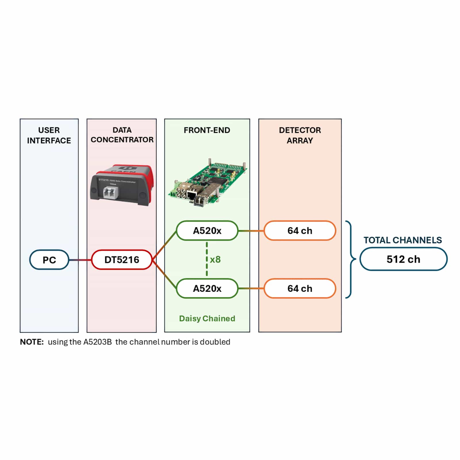
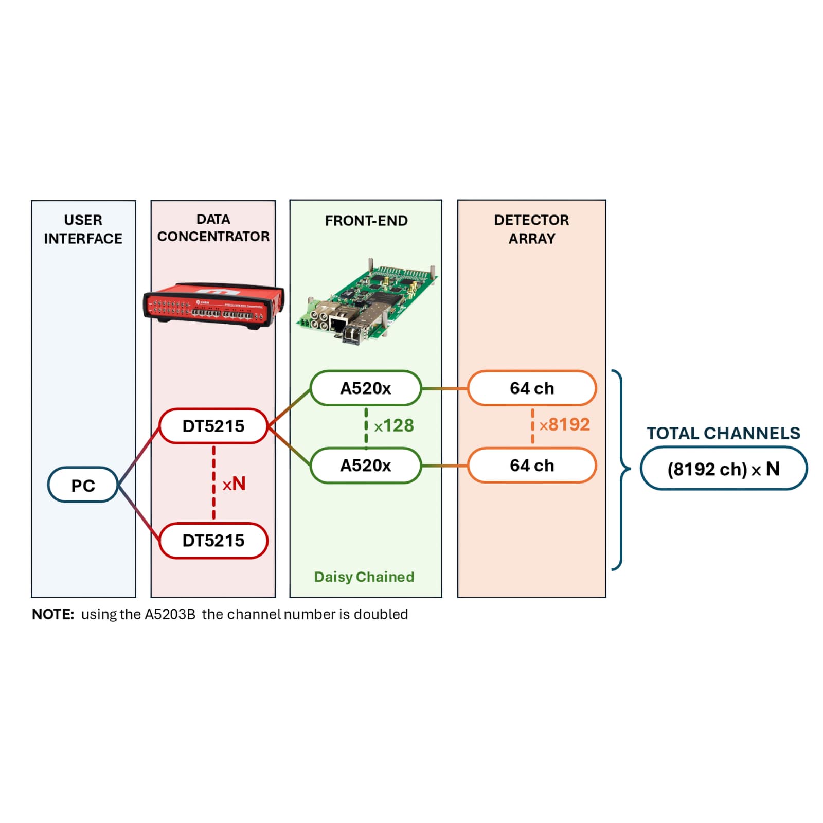
| USB2.0: microUSB connector Bandwidth = ∼ 3 MB/s | Ethernet connector, type Rj-45. Supports 10/100 Mbit/s connection to a PC Bandwidth = ∼ 2.5 MB/s | Small Form Factor Pluggable (SFP+) transceiver component for optical connection (3.125 Gbit/s). TDlink CAEN proprietary protocol allows for multi-board synchronization, slow control and data readout Data Concentrator DT5215 required |
| power supply voltage: +12 V (min = +7V, max = +15V) power consumption: t.b.d. 110V/220V AC/DC converter provided with Desktop version only. |
| Firmware of FPGA be upgraded via USB, Ethernet or Optical Link Firmware of μC can be upgraded via Ethernet only |
Readout SW
Fully controlled by the Janus 5205 open source software for Windows® and Linux®.
It can run in console mode (C program, with console commands and gnuplot display for plots) or connected to a GUI (Python) that implements user friendly configuration panels and run controls.
Janus 5205 can perform multiple board acquisition of PHA energy spectrum (Low and High Gain), ToT spectrum (represents PHA in timing mode), ΔT spectrum, with event building based on trigger ID or time stamp.
Live Display: channel hit count and rate, trigger rate, lost triggers, data throughput, acq. time, etc…
Plots: PHA, ΔT, ToT, hit rate, 2-D heat map with channel hit rates or PHA.
Threshold calibration curves via threshold scan (counts vs threshold)
Output Files: histograms (spectra), list files (PHA, ToA, ToT, ΔT), Run Info, Sync file.
Web Interface
Board information and monitoring, Ethernet configuration.
Compare with FERS-system.
Loading...
| Code | Description |
|---|---|
| WA5205XAAAAA | A5205 - 64 channel Psiroc unit for FERS-5200 with picoTDC RoHS |
PIN Diodes, Silicon Strips and GEMs Read-Out Chip
Concentrator Board for FERS-5200
64 Channel Radioroc unit for FERS-5200
Desktop 64 Channel picoTDC unit for FERS-5200
64 Channel Radioroc unit for FERS-5200
64/128 Channel picoTDC unit for FERS-5200
64 Channel Citiroc unit for FERS-5200
FERS-5200 DAQ SOFTWARE
High level library for FERS-5200 Boards
+39 0584 388 398
Contacts
What are you looking for?
Search