

3 Years Warranty

128 Channel Multihit TDC (100/200/800 ps)
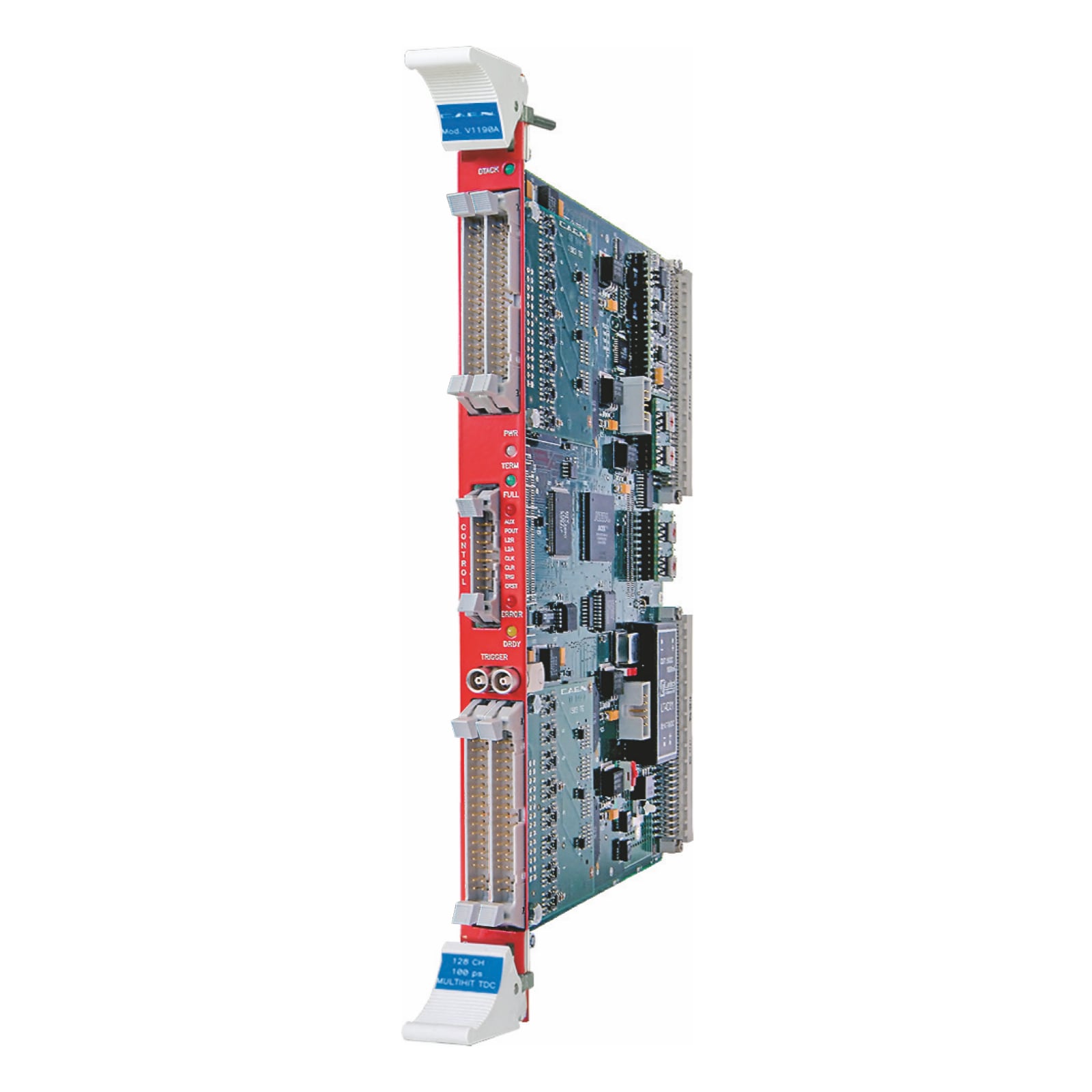
The CAEN Mod. VX1190A-2eSST is a 128 channel Multihit TDC, housed in a 1-unit wide VME64X 6U module. The unit features High Performance Time to Digital Converter chips developed by CERN. LSB can be set at 100 ps (19 bit resolution, 52 µs FSR), 200 ps (19 bit, 104 µs FSR) or 800 ps (17 bit, 104 µs FSR).
The channels can be enabled for the detection of hits rising/falling edges or for their width measurement (both the edges’ timing, and the hit width can be measured with the selected resolution). For each channel there is a digital adjustment for the zero-ing of any offsets. The data acquisition can be programmed in “Events” (“Trigger Matching Mode”, with a programmable time window) or in “Continuous Storage Mode”. Both ECL and LVDS input signals are supported. The module programming is performed via a microcontroller that implements a high-level user friendly interface. The VME interface allows the module to work in A24 and A32 addressing modes.
The board houses a 32 k x 32 bit deep Output Buffer that can be readout via VME in a completely independent way from the acquisition itself.
The device supports MBLT, CBLT and 2eSST readout modes. Live insertion is also supported.
6U-high, 1-unit wide, VMEx64X unit
128 ECL/LVDS inputs, 110 Ω impedance
Trigger Matching Mode, Continuous Storage Mode
5 ns
32 kwords deep Output Buffer
VME programmable: 100 / 200 / 800 ps
104 μs (200 ps and 800 ps LSB); 52 μs (100 ps LSB)
≤0.7 LSB
<2 ns7
Two LEMO 00 bridged connectors, NIM signal, 50 Ohm
75 ns
Internal (40 MHz) or External (on Control connector), dip switch selectable Control inputs active-high, differential ECL input signals:
CLR: performs the Hardware CLEAR (min. width: 25 ns)
rising-edge active, differential ECL input signals:
Compare with TDCs.
Loading...
| Code | Description |
|---|---|
| WVX1190AEXAE | VX1190A - 2ESST 128 Ch. Multievent Multihit TDC 100-200-800 psec ECL/LVDS (no JAUX) |
9U 21Slot VME64X Enhanced Crate series
8U 21 Slot VME64/64X Enhanced Crate Series
7U 21 Slot VME64 Low Cost Crate
7U 21 Slot VME64 Low Cost Crate
2U 4 Slot VME64 Mini Crate
1U 2 Slot VME64 Mini Crate
VME to USB 3.0/Ethernet/Optical Link Bridge
VME to USB 2.0 / Optical Link Bridge
7U CRATE VME/NIM 8 slot VME64 365W, 5 slot NIM 150W
Firmware Upgrade Tool for Front-end Boards Bridges & VME Power Supply
+39 0584 388 398
Contacts
What are you looking for?
Search