
Highlights
-
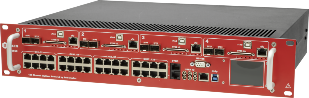
128 channels, 14-bit @125 MS/s Digitizer
-
Based on powerful Xilinx Zynq-7000 SoC with open FPGA
-
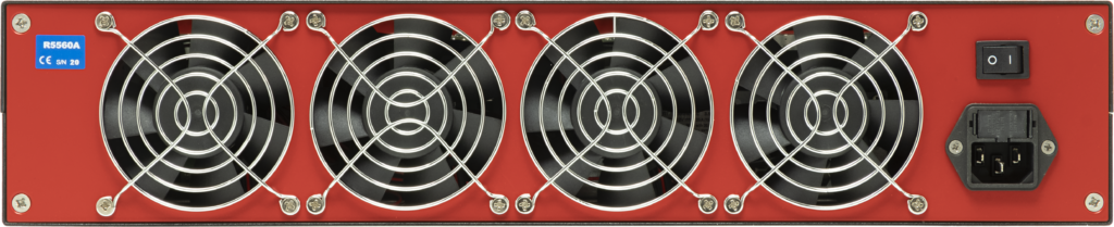
2U, 19” Rackmount unit with automatic fan control
-
Full-featured readout system for the readout of large arrays of detector (PMTs, segmented HPGe, Gas Tubes, …)
-
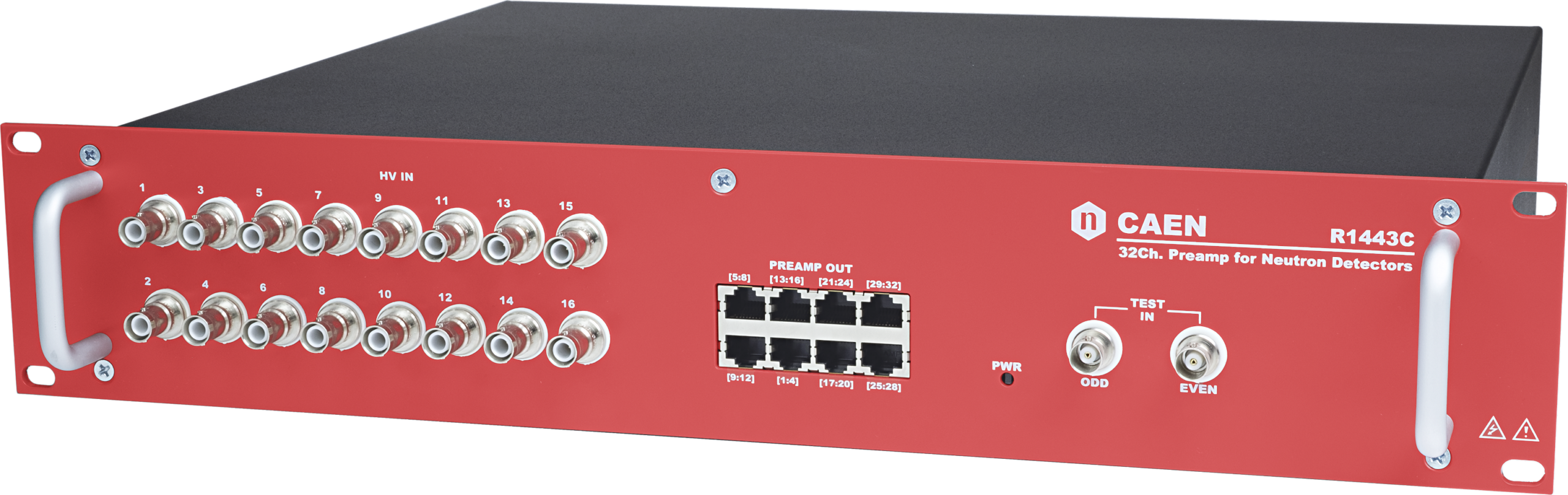
Specifically designed for the readout of position-sensitive 3He tubes in combination with R1443 preamplifier
-
2 Vpp input dynamic
-
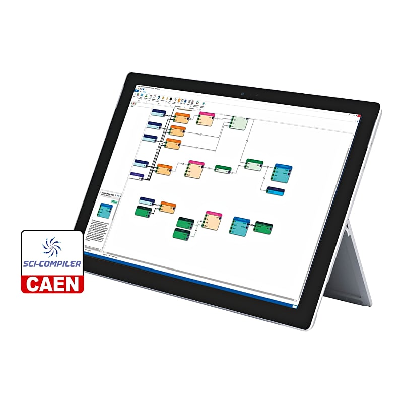
Fully supported by SCI-Compiler for easy FPGA programming (Firmware runtime license included onboard)
-
Easily scalable
-
Board-to-board synchronization with a single CAT5e cable.
-
Configurable digital I/Os to interface with external systems
-
Maximum flexibility: USB3.0, Ethernet, and Optical Link (OPTIONAL) connectivity, to support remote management as well as extreme fast data flow
-
2.4” touch screen display for quick configuration and status control
Overview
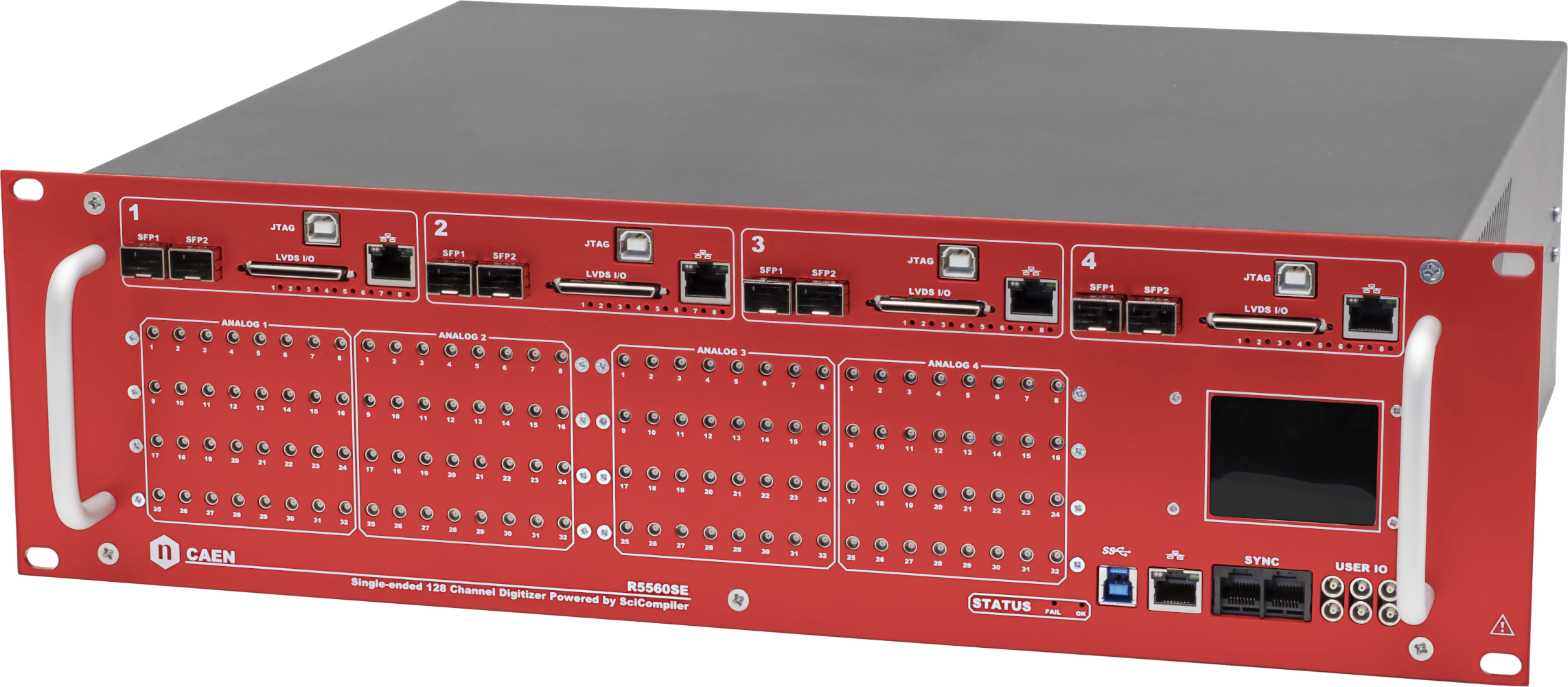
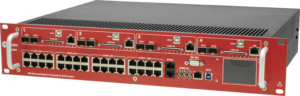
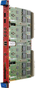
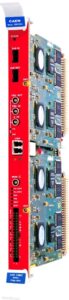
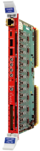
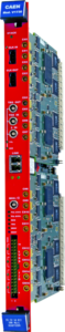
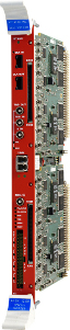
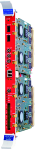
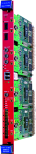
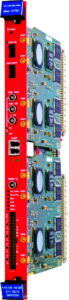
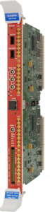
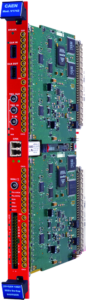
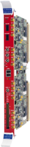
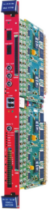
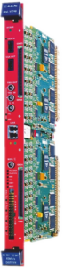
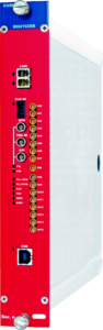
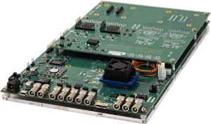
The R5560 is a 2U, 19″ rack-mount 128 Channels 14-bit 125MS/s Open FPGA Digitizer Family, designed to attain programmable data processing capabilities.
The R5560 is designed for the readout of large arrays of detectors (PMTs, segmented HPGe, 3He tubes, …) using a customizable platform. In fact, it is possible to take advantage of the powerful SoC mounted onboard to write a custom pulse processing algorithm on the open FPGA as well as build a middleware/software that fits the needs of the application of interest.
The board can manage simultaneously a large number of digital (LVDS, NIM, TTL) and analog signals, allowing to implement many functionalities required by physics experiments: signal digitization, complex trigger logic, Pulse Height Analysis with MCA capabilities, Time Tagging, Pulse Shape Discrimination, etc.
It is an optimal solution for large experiments, usually requiring fast digitization of analog signals and usage of several digital lines to interface with external systems. The board supports multi-board synchronization through a single CAT5e cable, with the possibility scale up to thousands of channels. Moreover, the rack-mount form factor simplifies the experimental setup in case of multi-board systems, where an effective space management is often a constraint. The usage of differential inputs on RJ45 connectors optimizes the cost for the installation, reducing the cabling cost.
SCI-Compiler software, the CAEN block-diagram-based firmware generator and compiler, helps in programming the FPGA to develop intensive real-time data processing. A free and open-source demo readout software is available to manage the standard pulse height analysis firmware implementing energy measurements using a trapezoidal filter.
Applications includes:
|
Readout of the following detectors |
|
|
Readout of mixed signals ASICs |
|
|
Nuclear Spectroscopy |
|
|
High Energy Physics |
|
|
Imaging with multichannel detectors |
Developed in collaboration with Nuclear Instruments.
You also may be interested in…
Request a Quote

Compare

|
Image
|
Name
|
Package
|
No. of Channels
|
Max Sampling Rate (MS/s)
|
Bandwidth (MHz)
|
Full Scale Range (V)
|
Resolution (bits)
|
Board Memory (Samples/ch)
|
Analog Input Connectors
|
CAEN firmware
|
Open FPGA
|
|
|
VX2730 |
VME64X |
32 |
500 |
250 |
[0.2 ÷ 4] |
14 |
84 M |
MCX |
DPP-PHA, DPP-PSD, D-SCOPE (cs) |
YES |
|
|
V1725 / V1725S |
VME |
8 / 16 |
250 |
125 |
0.5 - 2 |
14 |
640 k / 5.12 M |
MCX |
DPP-PHA, DPP-PSD, DPP-ZLEplus, D-WAVE |
NO |
|
|
DT2745 |
Desktop |
64 |
125 |
20 |
[0.04 + 4] |
16 |
21 M |
2mm 40-pin header male |
DPP-PHA, DPP-PSD, D-SCOPE, DPP-ZLEplus<sup>(cs)</sup> |
YES |
|
|
New R5560 |
rack mount 19 -2U |
128+6 |
125 |
60 |
2 |
14 |
max. 8k |
RJ45 |
n. a. |
YES |
|
|
New DTL2730 |
Desktop |
8 |
500 |
TBD |
TBD |
14 |
TBD |
MCX |
DPP-PHA(cs), DPP-PSD(cs), D-SCOPE(cs) |
YES |
|
|
V1761 |
VME |
2 |
4000 |
1000 |
1 |
10 |
7.2 M / 57.6 M |
MCX |
D-WAVE |
NO |
|
|
DT5751 |
Desktop |
2(DES mode) - 4 |
2000(DES mode) - 1000 |
500 |
0.2 / 1 |
10 |
3.6 M(DES mode) - 1.8 M |
MCX |
DPP-PSD, DPP-ZLEplus, D-WAVE |
NO |
|

|
VX1740D |
VME64X |
64 |
62.5 |
30 |
2 / 10 |
12 |
192 k |
SMC 68P |
DPP-QDC, D-WAVE |
NO |
|
|
DT5725 / DT5725S |
Desktop |
8 |
250 |
125 |
0.5 - 2 |
14 |
640 k / 5.12 M |
MCX |
DPP-PHA, DPP-PSD, DPP-ZLEplus, DPP-DAW, D-WAVE |
NO |
|
|
VX1724 |
VME64X |
8 |
100 |
40 |
0.5 / 2.25 / 10 |
14 |
512 k / 4 M |
MCX |
DPP-PHA, DPP-DAW |
NO |
|
|
DT5761 |
Desktop |
1 |
4000 |
1000 |
1 |
10 |
7.2 M |
MCX |
D-WAVE |
NO |
|
|
VX2745 |
VME64X |
64 |
125 |
20 |
[0.4 ÷ 4] |
16 |
21 M |
2mm 40-pin header male |
D-SCOPE, DPP-PHA, DPP-PSD, DPP-ZLEplus<sup>(cs)</sup> |
YES |
|
|
DT5724 |
Desktop |
4 / 2 |
100 |
40 |
0.5 / 2.25 / 10 |
14 |
512 k / 4 M |
MCX |
DPP-PHA, DPP-DAW, D-WAVE |
NO |
|
|
DT5730 / DT5730S |
Desktop |
8 |
500 |
250 |
0.5 - 2 |
14 |
640 k / 5.12 M |
MCX |
DPP-PHA, DPP-PSD, DPP-ZLEplus, DPP-DAW, D-WAVE |
NO |
|
|
VX2740 |
VME64X |
64 |
125 |
50 |
2 |
16 |
21 M |
2mm 40-pin header male |
DPP-PHA, D-SCOPE, DPP-PSD, DPP-ZLEplus<sup>(cs)</sup> |
YES |
|
|
V1724 |
VME |
8 |
100 |
40 |
0.5 / 2.25 / 10 |
14 |
512 k / 4 M |
MCX |
DPP-PHA, DPP-DAW, D-WAVE |
NO |
|
|
VX1761 |
VME64X |
2 |
4000 |
1000 |
1 |
10 |
7.2 M / 57.6 M |
MCX |
D-SCOPE |
NO |
|
|
DT2740 |
Desktop |
64 |
125 |
50 |
2 |
16 |
21 M |
2mm 40-pin header male |
DPP-PHA, DPP-PSD, D-SCOPE, DPP-ZLEplus<sup>(cs)</sup> |
YES |
|
|
V2740 |
VME |
64 |
125 |
50 |
2 |
16 |
21 M |
2mm 40-pin header male |
DPP-PHA, DPP-PSD, D-SCOPE, DPP-ZLEplus<sup>(cs)</sup> |
YES |
|
|
New DT2751 |
Desktop |
16 |
1000 |
500 |
[0.2 ÷ 2] |
14 |
84 M |
MCX |
DPP-PHA, DPP-PSD, D-SCOPE<sup>(cs)</sup> |
YES |
|
|
V1730 / V1730S |
VME |
8 / 16 |
500 |
250 |
0.5 - 2 |
14 |
640 k / 5.12 M |
MCX |
DPP-PHA, DPP-PSD, DPP-ZLEplus, D-WAVE |
NO |
|
|
N6725 / N6725S |
NIM |
8 |
250 |
125 |
0.5 - 2 |
14 |
640 k / 5.12 M |
MCX |
DPP-PHA, DPP-PSD, DPP-ZLEplus, DPP-DAW, D-WAVE |
NO |
|
|
New VX2751 |
VME64X |
16 |
1000 |
500 |
[0.2 ÷ 2] |
14 |
84 M |
MCX |
DPP-PHA, DPP-PSD, D-SCOPE<sup>(cs)</sup> |
YES |
|
|
VX1740 |
VME64X |
64 |
62.5 |
30 |
2 / 10 |
12 |
192 k / 1.5 M |
SMC 68P |
D-WAVE |
NO |
|
|
DT5740D |
Desktop |
32(SMC conn.) - 16(MCX conn) |
62.5 |
30 |
2 / 10 |
12 |
192 k |
SMC 68P - MCX |
DPP-QDC,D-WAVE |
NO |
|
|
V2745 |
VME |
64 |
125 |
20 |
[0.04 + 4] |
16 |
21 M |
2mm 40-pin header male |
DPP-PHA, DPP-PSD, D-SCOPE, DPP-ZLEplus<sup>(cs)</sup> |
YES |
|
|
DT5742 |
Desktop |
16 + 1 |
5000 (Based on DRS4 chip: 5 GS/s Switched Capacitor Array) |
500 |
1 |
12 |
0.128 / 1 |
MCX |
D-WAVE |
NO |
|
|
VX1725 / VX1725S |
VME64X |
8 / 16 |
250 |
125 |
0.5 - 2 |
14 |
640 k / 5.12 M |
MCX |
DPP-PHA, DPP-PSD, DPP-ZLEplus, DPP-DAW, D-WAVE |
NO |
|
|
VX1730 / VX1730S |
VME64X |
8 / 16 |
500 |
250 |
0.5 - 2 |
14 |
640 k / 5.12 M |
MCX |
DPP-PHA, DPP-PSD, DPP-ZLEplus, DPP-DAW, D-WAVE |
NO |
|
|
V2730B |
VME64 |
16 |
500 |
250 |
[0.2 ÷ 4] |
14 |
84 M |
MCX |
DPP-PHA, DPP-PSD, D-SCOPE(cs) |
YES |
|
|
N6730 / N6730S |
NIM |
8 |
500 |
250 |
0.5 - 2 |
14 |
640 k / 5.12 M |
MCX |
DPP-PHA, DPP-PSD, DPP-ZLEplus, DPP-DAW, D-WAVE |
NO |
|
|
V1743 |
VME |
16 |
3200 (Based on SAMLONG chip: 3.2 GS/s Switched Capacitor Array) |
500 |
2.5 |
12 |
0.007 M |
MCX |
D-WAVE |
NO |
|
|
VX1751 |
VME64X |
2(DES mode) - 4 |
2000(DES mode) - 1000 |
500 |
0.2 / 1 |
10 |
3.6 M(DES mode) - 1.8 M / 28.8 M(DES mode) - 14.4 M |
MCX |
DPP-PSD, DPP-ZLEplus, D-WAVE |
NO |
|

|
DT5740 |
Desktop |
32(SMC conn.) - 16(MCX conn) |
62.5 |
30 |
2 / 10 |
12 |
192 k |
SMC 68P - MCX |
D-WAVE |
NO |
|
|
V1720 |
VME |
8 |
250 |
125 |
2 |
12 |
1.25 M / 10 M |
MCX |
DPP-PSD, D-WAVE |
NO |
|
|
V1751 |
VME |
2(DES mode) - 4 |
2000(DES mode) - 1000 |
500 |
0.2 / 1 |
10 |
3.6 M(DES mode) - 1.8 M / 28.8 M(DES mode) - 14.4 M |
MCX |
DPP-PSD, DPP-ZLEplus, D-WAVE |
NO |
|
|
VX1742 |
VME64X |
32 + 2 |
5000 (Based on DRS4 chip: 5 GS/s Switched Capacitor Array) |
500 |
1 |
12 |
0.128 / 1 |
MCX |
D-WAVE |
NO |
|
|
DT5743 |
Desktop |
8 |
3200 (Based on SAMLONG chip: 3.2 GS/s Switched Capacitor Array) |
500 |
2.5 |
12 |
0.007 M |
MCX |
D-WAVE |
NO |
|
|
DT5720 |
Desktop |
4 / 2 |
250 |
125 |
2 |
12 |
1.25 M / 10 M |
MCX |
DPP-PSD, D-WAVE |
NO |
|
|
V1742 |
VME |
32 + 2 |
5000 (Based on DRS4 chip: 5 GS/s Switched Capacitor Array) |
500 |
1 |
12 |
0.128 / 1 |
MCX |
D-WAVE |
NO |
|
|
DT2730 |
Desktop |
32 / 16 |
500 |
250 |
[0.2 ÷ 4] |
14 |
84 M |
MCX |
DPP-PHA, DPP-PSD, D-SCOPE |
YES |
|
|
VX1743 |
VME64X |
16 |
3200 (Based on SAMLONG chip: 3.2 GS/s Switched Capacitor Array) |
500 |
2.5 |
12 |
0.007 M |
MCX |
D-WAVE |
NO |
|
|
V1740D |
VME |
64 |
62.5 |
30 |
2 / 10 |
12 |
192 k |
SMC 68P |
DPP-QDC, D-WAVE |
NO |
|
|
New DTL2751 |
Desktop |
4 |
1000 |
TBD |
TBD |
14 |
TBD |
MCX |
DPP-PSD(cs), D-SCOPE(cs) |
YES |
|
|
VX1720 |
VME64X |
8 |
250 |
125 |
2 |
12 |
1.25 M / 10 M |
MCX |
DPP-PSD, D-WAVE |
NO |
|
|
N6742 |
NIM |
16 + 1 |
5000 (Based on DRS4 chip: 5 GS/s Switched Capacitor Array) |
500 |
1 |
12 |
0.128 / 1 |
MCX |
D-WAVE |
NO |
Technical Specifications
|
General |
Form Factor : 19”, 2U Rack-mount |
|
Power Requirements |
Voltage: 100-240 Vac |
|
Analog Input |
|
|
Digital Input |
|
|
Digital Conversion |
|
|
Clock Generation |
Clock source: internal/external |
|
LEMO Digital I/O |
USER IO 0…5 (LEMO)
|
|
Trigger |
Trigger Source: Internal/External: managed by the default firmware; Complex trigger logic: implementable by the user on the open FPGA. |
|
Open FPGA |
4x Xilinx Zynq-7000 SoC: |
|
Memory |
1 GByte of memory for list readout on each SoC |
|
Communication Interface |
All readout interfaces allow to perform the same task at different speed and using different media. They can be used independently or simultaneously.
|
|
Firmware |
Default: Waveform recording and Pulse Height Analysis, Ethernet communication |
|
Firmware Upgrade |
Firmware can be upgraded via Ethernet, USB 3.0 or USB 2.0 debugger (on-fly) |
|
Software |
|
Footer