

3 Years Warranty
3 Years Warranty

128 Channels Latching Scaler for V2495 and DT5495
Free downloadable FW2495SC Trial version.
|
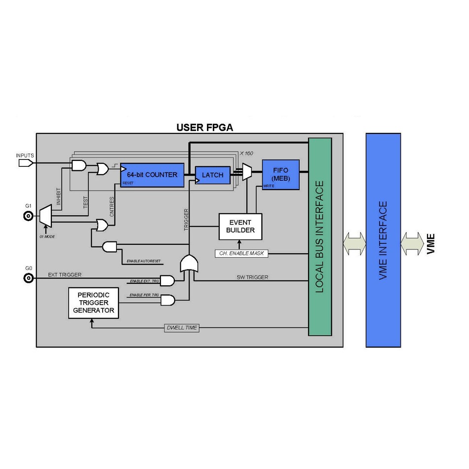
FW2495SC is a FPGA firmware for CAEN V2495 and DT5495 models that allows to use the board as a Multievent latching scaler housing up to 160 independent counting channels (the maximum number of channels is achieved if the V2495/DT5495 is expanded with three A395A boards). Each channel has a programmable 32 or 64 bit counting depth and accepts LVDS/ECL/PECL inputs; up to 200 MHz of counting frequency is supported.
Each counter is incremented at the leading edge of the input signal. As a trigger arrives, all counters are latched simultaneously and independently from the counting operations, that continue unaffected. Thanks to a synchronization technique, the counter value is significant, even when it is incremented during the readout.
After the latched counter values have been made available for readout, the FPGA writes them into a FIFO memory (Multi Event Buffer or MEB) together with a data header and, optionally, the active channel masks. Events written in the MEB can be readout via VME. Once an event has been written, the Scaler can accept another trigger even if the previous event has not been readout yet, provided that the FIFO memory has enough space left for other data.
The trigger signal can be either fed to the G0 connector (NIM or TTL) or internally generated by the FPGA, with a specific trigger period (DWELL TIME) ranging from 1μs to 4000 s in 1-μs steps, or can be sent via VME, by a write access to a specific register. Trigger Time tag information can be programmed to be included in the event as a 32 or 64-bit format.
The lowest 32 bits of the counter values can be also read via VME on the fly, independently from the counting, trigger and event recording operations.
The G1 connector can be alternatively used as Counting Inhibit, Test signal (parallel counting) or Counters reset.
The counters reset can be also asserted every time a trigger is sent (auto-reset option); in this way, the read values represent the counting value between two consecutive triggers instead of the absolute counting values since the board switch-on (or its last reset). The counters can also be reset via VME command.
The FW2495SC firmware features a configurable legacy option of the event payload, so that acquisition systems developed for the V1495 can be compatible with V2495.
V2495Scaler Demo Software
CAEN provides a Windows-compliant demo application as an introduction to the principles of operation of the FW2495 firmware. By means of a configuration text file managed by the demo, it is possible to set the main functions. The included C source files and Visual Studio project offer a good model for developing customized software solutions. The demo is manageable by VME and is also compatible with V1495 boards when the event payload legacy option is enabled.
Compare with DPP.
Loading...
| Code | Description |
|---|---|
| WFW2495SCXAA | FW2495SC - 160 Channels Latching Scaler for V2495 and DT5495 |
Interface library for CAEN Data Acquistion Modules
+39 0584 388 398
Contacts
What are you looking for?
Search