

3 Years Warranty
3 Years Warranty
3 Years Warranty

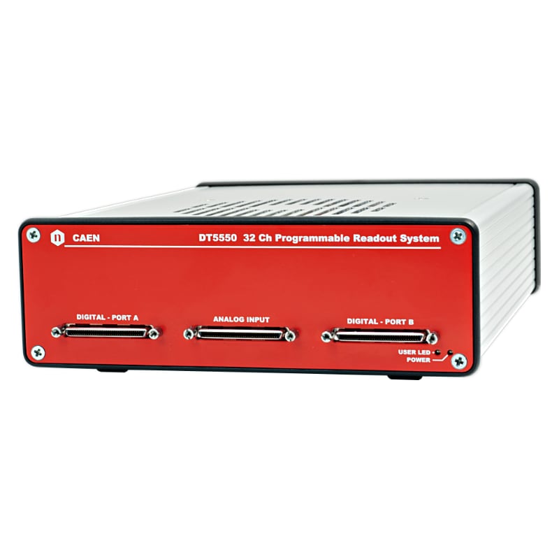
32 Channel Programmable Readout System
The CAEN Mod. DT5550 is a Programmable 32-channel Sequencer and Readout System for physics application. It is one of the CAEN programmable board compatible with SCI-Compiler, the innovative software tool for easy FPGA programming, designed to help users in building a customized DAQ. The default firmware, the demo readout software and some design files are distributed for free and open source, allowing the user to minimize the effort in designing the DAQ.
The DT5550 is capable to manage simultaneously a large number of digital and differential analog signals, making it suitable to readout most of the ASICs commonly used in physics applications.
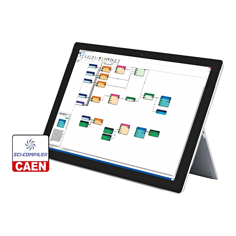
The DT5550 is fully supported by SCI-Compiler, a Windows-based graphical development system for block-diagram-based FPGA programming. This tool allows to develop and compile the firmware code using graphical blocks which represents the functionalities needed for firmware implementation (for example oscilloscope, TDC, MCA, charge integration, etc). SCI-Compiler automatically generates the VHDL firmware code starting only from logic blocks and virtual instruments that can be connected together in the GUI and, moreover, it generates C/C++/C#/Python Libraries for custom software development in Windows and Linux.
A complete, ready to use default firmware is provided for free and open source. The default firmware manages the basic waveform digitization and charge integration and it is preloaded on the board. The user can open the default firmware in SCI-Compiler and modify it in order to customize, for example, the trigger logic, the data online processing or integrate it in a larger system.
The SCI-Compiler license and one-year free upgrade is included with the DT5550.
The SCI-55×0 Readout Software is the free and open source Windows-based software developed to perform basic acquisitions with the DT5550. It works in conjunction with the DT5550 default firmware and it can be modified by the user according to the custom functions implemented in the firmware and for any other need.
Available board models and accessories are listed in the tab “ordering option” and “accessories”.
Developed in collaboration with
163 x 50 x 226 mm3 (WxHxD) Desktop
Channels: 32 Channels, Differential
Connector: VHDCI
Bandwidth: 31 MHz
Impedance: Zdiff = 100 Ω
Full Scale Range: 2 Vpp
Channels: 2 x 24 channels, Differential
Connector: 2 x VHDCI
Signal Type: CMOS 3.3V, LVCMOS 1.8V, LVDS, BLVDS
Impedance: Zdiff = 100 Ω
Coupling: AC
Resolution: 14 bits
Sampling Rate: 80 MS/s Simultaneously on each channel
Clock source: internal/external
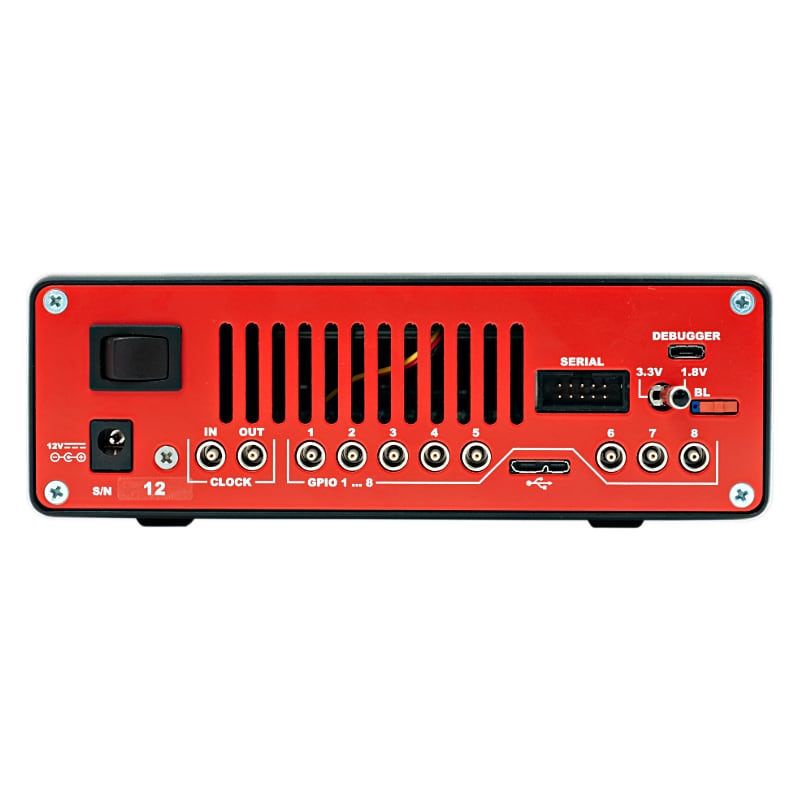
On-board programmable PLL provides generation of the main board clocks from an internal (25 MHz local Oscillator) or external (rear panel CLK-IN connector) reference
16 kS/ch
Trigger Source
Internal/External: managed by the default firmware
Complex trigger logic: implementable by the user on the open FPGA
Trigger Propagation
Through programmable LEMO GPIO 1 – 8
Trigger Time Stamp
Default FW: 32-bit counter, 12.5 ns resolution, 50 s range;
Custom FW: defined by the firmware design
Clock Propagation
LEMO CLOCK IN/OUT connectors
Acquisition Synchronization
Through programmable LEMO GPIO 1 – 8
Open FPGA
Xilinx XC7K160T (Kintex-7 family)
USB 3.0
USB 2.0 back compatibility Up to 240 MB/s transfer rate
Firmware can be upgraded via USB 3.0 or mini-USB debugger (on-fly)
Compare with Programmable DAQ Platforms.
Loading...
| Code | Description |
|---|---|
| WDT5550XAAAA | DT5550 - 32 Channel DAQ System with Programmable FPGA and Sequencer RoHS |
Single Ended to Differential Input Adapter for DT5550
Multi-Functional Software Suite for the Upgrade of Front-end Boards, Bridges and Power Supplies
+39 0584 388 398
Contacts
What are you looking for?
Search