

3 Years Warranty

Low Noise Fast Rise Time Charge Sensitive Preamplifiers
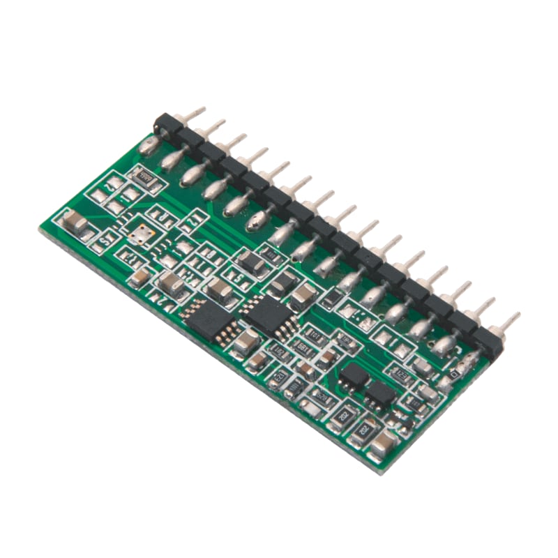
The CAEN Mod.A1422H series are charge sensitive preamplifiers implemented on a single-in-line package. Various sensitivity values are available and various detectors capacitances are supported:
Two version of A1422H modules are available:
All of them can be used in nuclear and subnuclear physics experiments, where very low noise, fast response and high counting rates are required. The modules accept both positive and negative input charge pulses and provide an energy output of ±3.5 V / ±4 V (Hybrid / PCB) range on 50 Ω termination (±8 V / ±10 V on 1 kΩ). Moreover, a test input accepts positive and negative signals for calibration purposes.
The hybrid preamplifiers are realized using a Cold Discharge Mechanism: this allows to have a low decay time value maintaining a very high feed resistance value. This technique provides good performances minimizing the pile-up in presence of moderate high counting rates.
CAEN offers charge sensitive preamplifiers (Mod. A1422) based on A1422H modules and packaged in a 1/4/8 channels boxes. A1422 are implemented into alloy boxes and feature SHV connectors for the IN/DETECTOR and HV BIAS signals, LEMO connectors for the TEST IN and ENERGY OUT and a cable with a D-type 9 pin male connector for the power supply.
Single in-line package hybrid (38 mm x 23 mm x 3 mm)
pin pitch: 2.54 mm; weight: 2.63 g
1
Accepts positive and negative charge pulses from semiconductor detectors and supplies the HV bias to the detector itself
Hybrid: Up to 200 V (positive or negative) – 100 MΩ resistance in series
PCB: Up to 800 V (positive or negative) – 10 MΩ resistance in series
Positive or negative inputs for the energy calibration via Ctest= 1 pF (or 10 pF; sensitivity: 5 mV/MeV)
Hybrid: ± 8V max. (open circuit), 50 Ω back termination.
PCB: ± 10V max. (open circuit), 50 Ω back termination.
Hybrid: <± 0.05% (0 ÷ ±8 V 1 kΩ termination)
PCB: <± 0.05% (0 ÷ ±10 V 1 kΩ termination)
< ±100 ppm/°C (0 to 50°C)
5/45/90/400/450 mV/MeV
+12 V: F2:14 mA – F3: 24 mA
-12 V: F2: 6 mA – F3: 6 mA
+12 V: F2:12 mA – F3: 20 mA
-12 V: F2: 4 mA – F3: 4 mA
Compare with:
Loading...
| Code | Description |
|---|---|
| WA1422H005F2 | A1422H005F2 - Charge Preamplifier Module, 5mV/MeV gain, Cdet<200pF RoHS |
| WA1422H005F3 | A1422H005F3 - Charge Preamplifier Module, 5mV/MeV gain, Cdet<1000pF RoHS |
| WA1422H045F2 | A1422H045F2 - Charge Preamplifier Module, 45mV/MeV gain, Cdet<200pF RoHS |
| WA1422H045F3 | A1422H045F3 - Charge Preamplifier Module, 45mV/MeV gain, Cdet<1000pF RoHS |
| WA1422H090F2 | A1422H090F2 - Charge Preamplifier Module, 90mV/MeV gain, Cdet<200pF RoHS |
| WA1422H090F3 | A1422H090F3 - Charge Preamplifier Module, 90mV/MeV gain, Cdet<1000pF RoHS |
| WA1422H400F2 | A1422H400F2 - Charge Preamplifier Module, 400mV/MeV gain, Cdet<200pF RoHS |
| WA1422H001F3 | A1422H001F3 - Charge Preamplifier Module, 1mV/MeV gain, Cdet<1000pF RoHS |
| WA1422H450F2 | A1422H450F2 - Charge Preamplifier Module, 450mV/MeV gain, Cdet<200pF RoHS |
Low Noise Fast Rise Time Charge Sensitive Preamplifiers (Boxed)
+39 0584 388 398
Contacts
What are you looking for?
Search