
-
10 bit @ 2 GS/s (interleaved) or 1 GS/s
-
Analog input on MCX coaxial connector (50 Ω, single-ended)
-
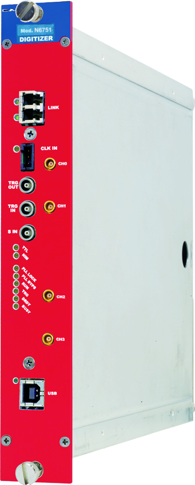
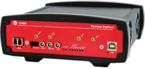
2-4 channels, NIM module
-
1 Vpp input dynamic range (0.2 Vpp on request) with programmable DC offset
-
Algorithms for Digital Pulse Processing:
-
Time-stamped Waveform and List
-
USB and Optical Link communication interfaces
-
Multi-board synchronization features
-
Daisy chain capability
-
Compliant with CoMPASS, DPP-ZLEplus Demo Software, CAENScope, CAEN WaveDump, C and LabVIEW libraries
The CAEN Mod.N6751 is a digitizer able to record waveforms along with performing advanced algorithms for online digital pulse processing (DPP) of charge integration and pulse shape discrimination with constant fraction timing and zero-length encoding.
Data is read by a Flash ADC, 10-bit resolution and 1 GS/s sampling rate (2 GS/s using half of the channels in DES mode*), which is well suited for fast signals as the ones coming from fast organic, inorganic and liquid scintillators coupled to PMTs or Silicon Photomultipliers, Diamond detectors and others. The acquisition can be channel independent and it is possible to make coincidence/anti-coincidence logic among different channels and external veto/gating. Multiple boards can be synchronized to build up complex systems.
In the case of DPP mode, data can be saved in time-stamped list mode to support higher input rates and improve the throughput performances.
Piled-up events can be rejected or saved for offline analysis. The acquisition in DPP mode is fully controlled by the CoMPASS software, which manages the algorithm parameters, builds, plots and saves the relevant energy, time, and PSD spectra. In the case of waveform recording mode, the user can take advantage of the CAENScope and WaveDump software to access and save the waveforms.
Libraries and demo software in C and LabView are available for integration and customization of specific acquisition systems.
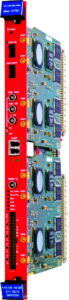
The N6751 comes in a NIM form factor with 2/4 input channels (2 channels in case of DES mode*). The communication to and from the board is provided through USB and Optical Link interfaces.
(*) NOTE: DES mode is not available with DPP firmware


Accessories
A318
A317
AI2700
A654
A659
You also may be interested in…
Request a Quote

Compare

|
Image
|
Name
|
Package
|
No. of Channels
|
Max Sampling Rate (MS/s)
|
Bandwidth (MHz)
|
Full Scale Range (V)
|
Resolution (bits)
|
Board Memory (Samples/ch)
|
Analog Input Connectors
|
CAEN firmware
|
Open FPGA
|
|
|
DT5751 |
Desktop |
2(DES mode) - 4 |
2000(DES mode) - 1000 |
500 |
0.2 / 1 |
10 |
3.6 M(DES mode) - 1.8 M |
MCX |
DPP-PSD, DPP-ZLEplus, D-WAVE |
NO |
|
|
VX1751 |
VME64X |
2(DES mode) - 4 |
2000(DES mode) - 1000 |
500 |
0.2 / 1 |
10 |
3.6 M(DES mode) - 1.8 M / 28.8 M(DES mode) - 14.4 M |
MCX |
DPP-PSD, DPP-ZLEplus, D-WAVE |
NO |
|
|
V1751 |
VME |
2(DES mode) - 4 |
2000(DES mode) - 1000 |
500 |
0.2 / 1 |
10 |
3.6 M(DES mode) - 1.8 M / 28.8 M(DES mode) - 14.4 M |
MCX |
DPP-PSD, DPP-ZLEplus, D-WAVE |
NO |
Technical Specifications
|
GENERAL |
16 general purpose LVDS I/O controlled by the FPGA: Run, Busy, Veto, Trigger and other functions can be programmed |
|
ANALOG INPUT |
Firmware can be upgraded via VMEbus or Optical Link |
|
DIGITAL CONVERSION |
General purpose C libraries, configuration tools, readout software (Windows® and Linux® support), LabVIEW™ VIs and demos for Windows® only |
|
SYSTEM PERFORMANCES |
5.6 A @ +5V; 250 mA @ +12V, -12V not used |
|
ADC CLOCK GENERATION |
Form Factor Weight |
|
DIGITAL I/O |
Channels Connector Abs Max Rating |
|
ACQUISITION MEMORY |
Resolution Sampling Rate |
|
TRIGGER |
|
|
SYNCHRONIZATION |
|
|
ADC & MEMORY CONTROLLER FPGA |
CLK-IN (AMP Modu II) GPO (LEMO) TRG-IN (LEMO) |
|
COMMUNICATION INTERFACE |
1.835 MS/ch (1.9 ms @ 1GS/s) or 3.6 MS/ch in DES mode (1.9 ms @ 2GS/s); 14.4 MS/ch (15 ms @ 1 GS/s) or 28.8 MS/ch in DES mode (15 ms @ 2 GS/s) divisible into 1 ÷ 1024 buffers |
|
FIRMWARE |
Trigger Source Trigger Time Stamp |
|
SOFTWARE |
Clock Propagation Acquisition Synchronization Trigger Time Stamp Alignment |
|
POWER CONSUMPTIONS |
Two Altera Cyclone EP3C16 (one FPGA serves 2 channels) |
Footer