

Highlights
-
12 bit 62.5 MS/s ADC
-
32 channels (16 channels on LEMO connectors using A746D adapter)
-
ERNI SMC Dual Row 68 pin connector (32 channels)
-
2 Vpp single ended input range
-
16-bit programmable DC offset adjustment: ±1 V
-
Trigger Time stamps
-
Memory buffer: 192 kS/ch, up to 1024 events
-
FPGA for real-time data processing:
-
Programmable event size and pre-post trigger adjustment
-
Optical Link interface (CAEN proprietary protocol)
-
USB2.0 interface
-
Firmware upgradeable via USB/Optical Link
-
Libraries, Demos (C and LabView) and Software tools for Windows and Linux
Overview
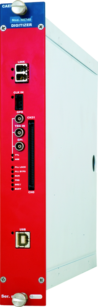
The N6740D is a 32ch 12 bit 62.5 MS/s (65 MS/s using external clock) NIM Waveform Digitizer with 2 Vpp single ended input dynamics on a ERNI SMC connector. 32 channels can be available on LEMO connectors using the A746D adapter.
The DC offset adjustment (range ±1 V) by a programmable 16bit DACs (one for each 8-channel group) allows a right sampling of a bipolar (Vin = ±1 V) up to a full positive (Vin = 0 ÷ +2 V) or negative (Vin= 0 ÷ -2 V) analog input swing without losing dynamic resolution.
The module features a front panel Clock Input and a PLL for clock synthesis from internal/external references. The data stream is continuously written in a circular memory buffer. When the trigger occurs, the FPGA writes further N samples for the post trigger and freezes the buffer that can be read by USB or Optical Link. The acquisition can continue without dead time in a new buffer.
Each channel has a SRAM Multi-Event Buffer of 192 kS divisible into 1 ÷ 1024 buffers of programmable size. The readout (by USB or Optical Link) of a frozen buffer is independent from the write operations in the active circular buffer (ADC data storage).
N6740D supports multi-board synchronization allowing all ADCs to be synchronized to a common clock source and ensuring Trigger time stamps alignment. Once synchronized, all data will be aligned and coherent across multiple N6740 boards.
The trigger signal can be provided externally via the front panel Trigger Input as well as via the software, but it can also be generated internally thanks to threshold self-trigger capability.
N6740D houses USB 2.0 and Optical Link interfaces. USB 2.0 allows data transfers up to 30 MB/s. The Optical Link supports transfer rate of 80 MB/s and offers Daisy chain capability. Therefore, it is possible to connect up to 8/32 ADC modules to a single Optical Link Controller (Mod. A2818).
Software available (Windows and Linux):
CAEN provides drivers for all the different types of physical communication channels, a set of C and LabView libraries (CAENComm and CAENDigitizer), demo applications and utilities:
-
CAENUpgrader: tool that allows the user to update the firmware of the digitizers, change the PLL settings, load, when requested, the license for the pay firmware and other utilities.
Standard Firmware compliant:
-
CAEN WaveDump: software console application that can be used to configure and readout event data from any model of the CAEN digitizer family and save the data into a memory buffer allocated for this purpose.
Digital Pulse Processing firmware for Physics Applications – this special firmware allows to perform on-line processing on detector signal directly digitizer:
-
DPP-QDC Pulse Processing for Charge to Digital Converter DT5740D digitizer running DPP-QDC firmware becomes a digital replacement of Single Gate QDC plus Discriminator and Gate Generator.
-
CoMPASS Multiparametric Acquisition Software.
Accessories
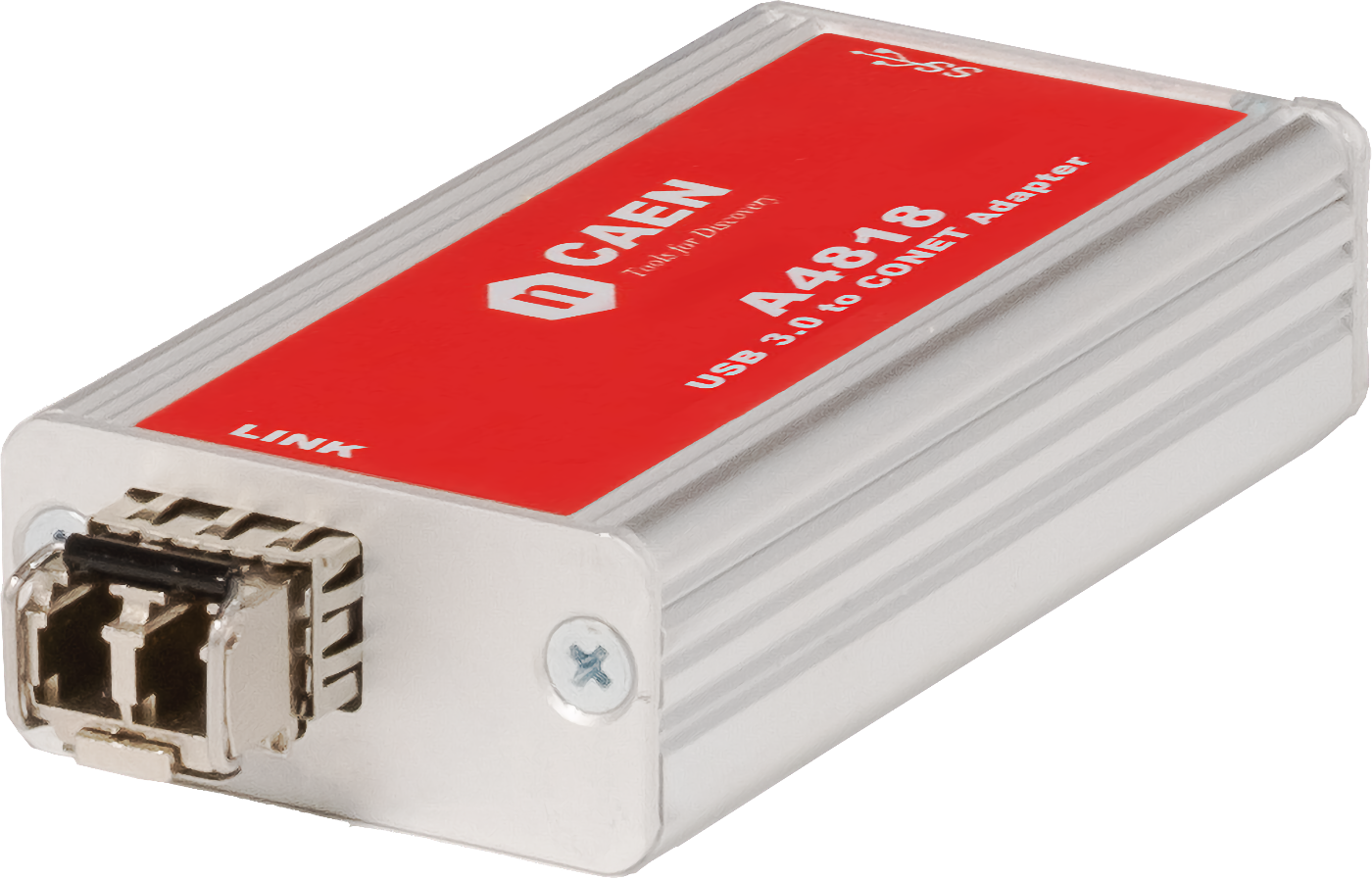
A4818
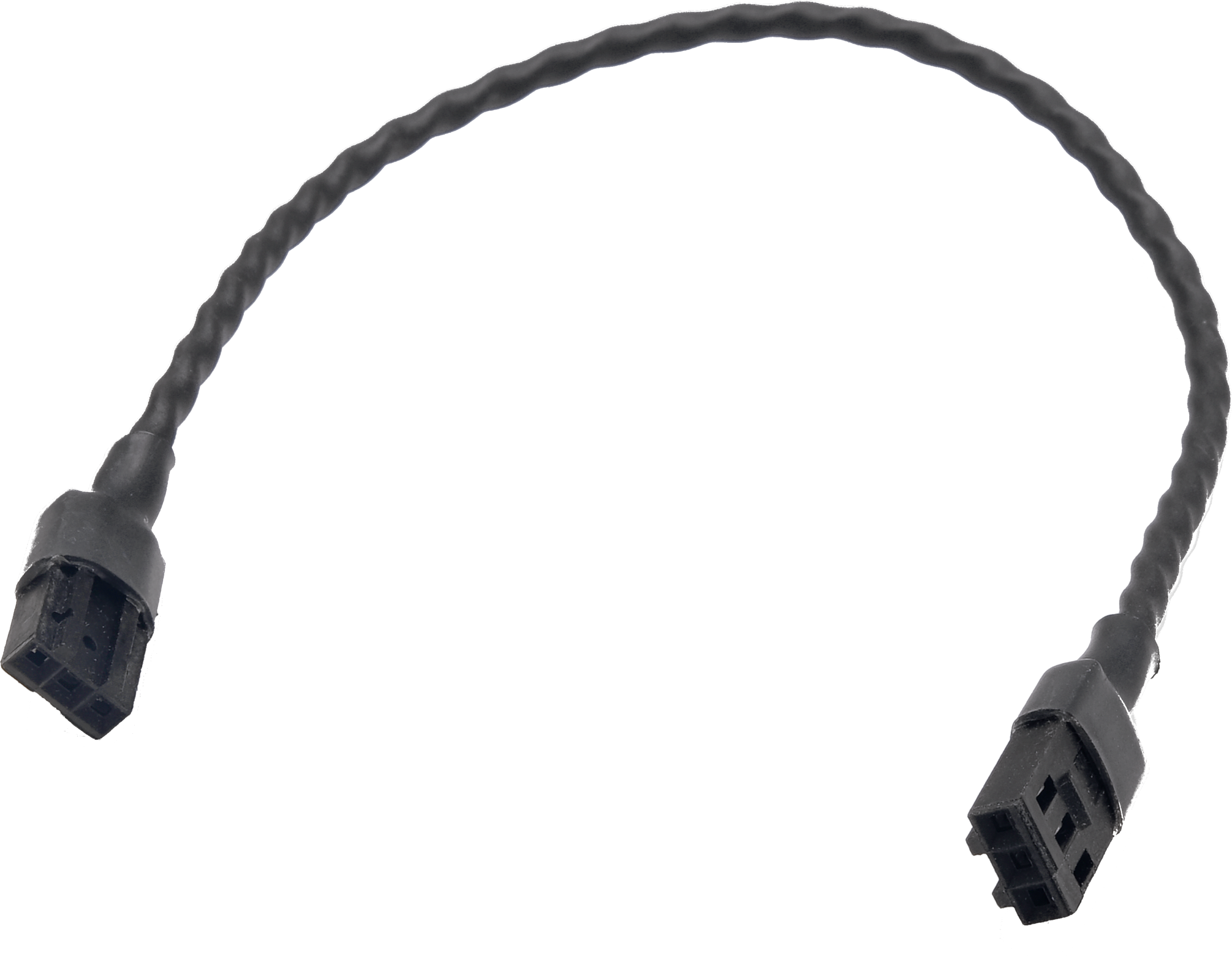
A317
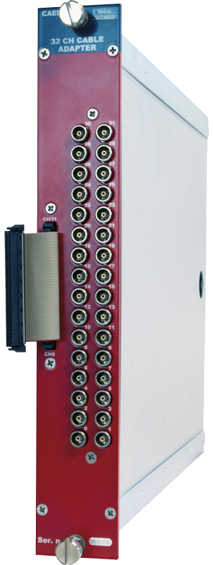
A746D
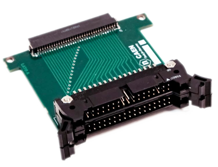
A371
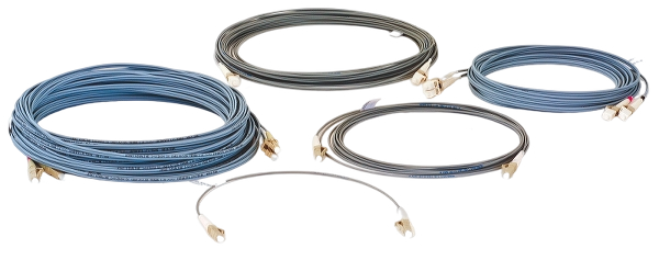
AI2700
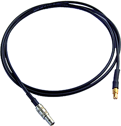
A654
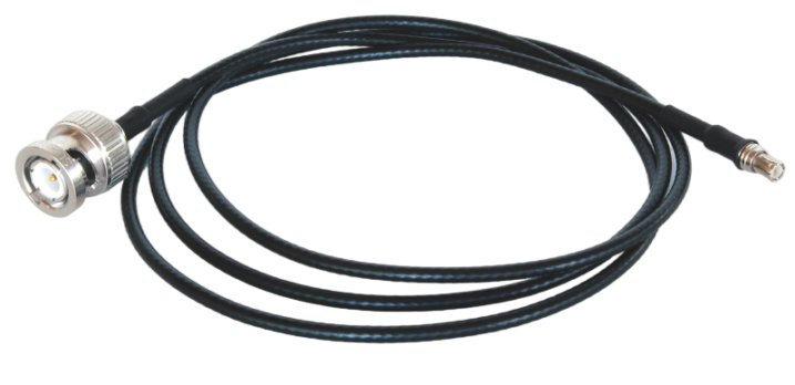
A659
You also may be interested in…
A4818
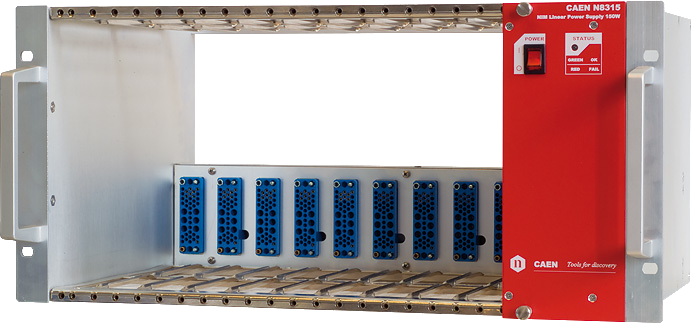
NIM8302
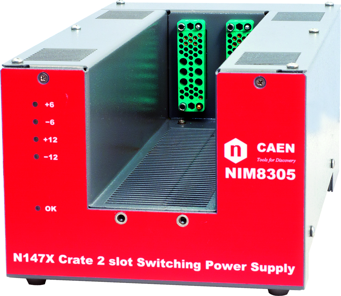
NIM8305
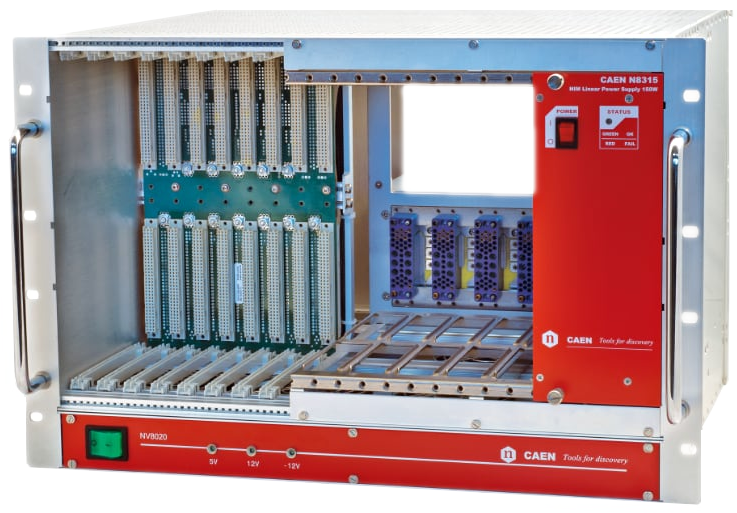
NV8020A
NIM8303
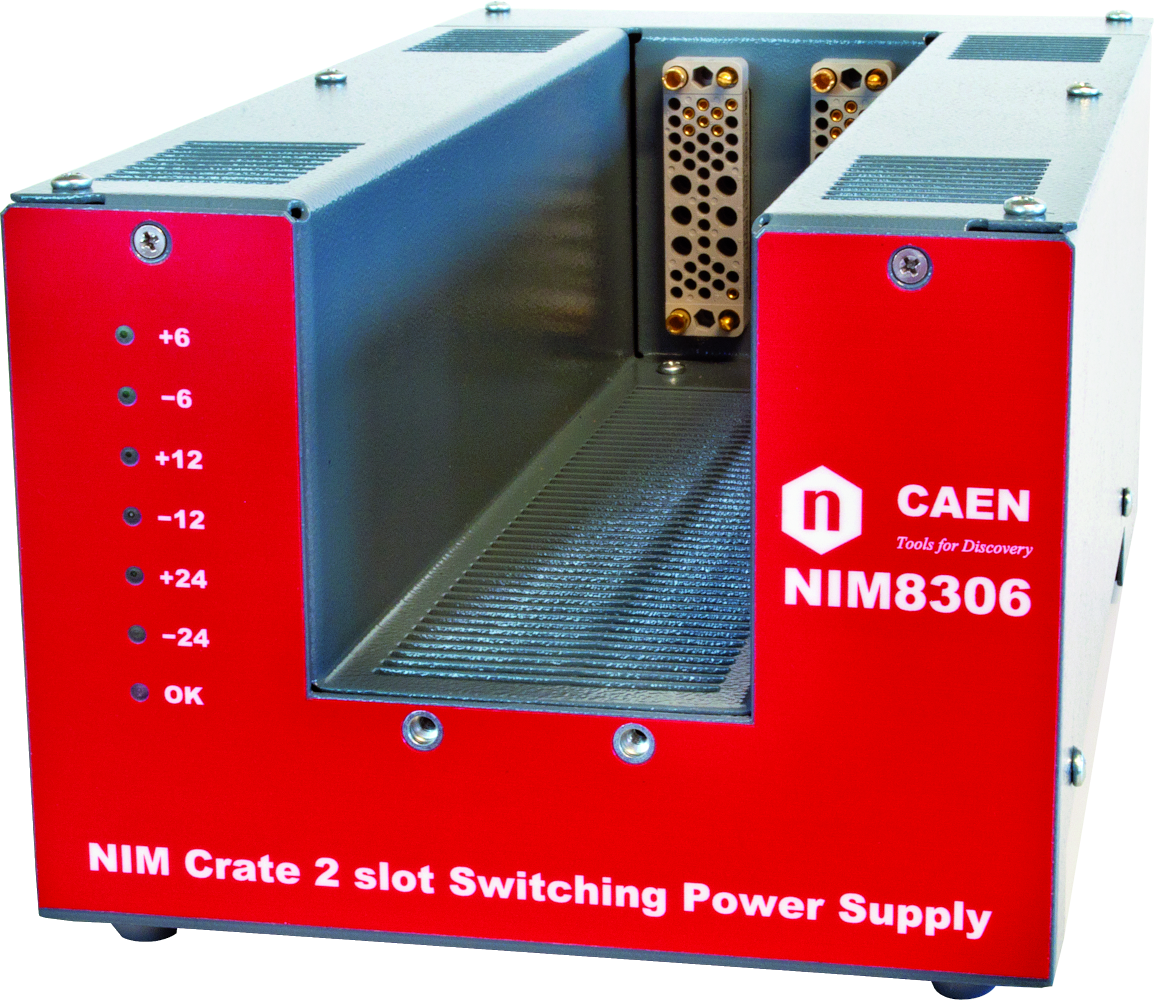
NIM8306
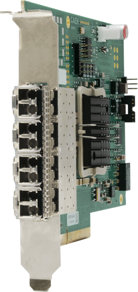
A5818
Request a Quote

Compare

|
Image
|
Name
|
Resolution (bits)
|
Max Sampling Rate (MS/s)
|
No. of Channels
|
Package
|
Bandwidth (MHz)
|
Full Scale Range (V)
|
Board Memory (Samples/ch)
|
Analog Input Connectors
|
CAEN firmware
|
Open FPGA
|
|
|
VX2730 |
14 |
500 |
32 |
VME64X |
250 |
[0.2 ÷ 4] |
84 M |
MCX |
DPP-PHA, DPP-PSD, D-SCOPE (cs) |
YES |
|
|
V1725 / V1725S |
14 |
250 |
8 / 16 |
VME |
125 |
0.5 - 2 |
640 k / 5.12 M |
MCX |
DPP-PHA, DPP-PSD, DPP-ZLEplus, D-WAVE |
NO |
|
|
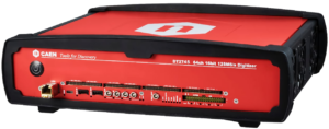
DT2745 |
16 |
125 |
64 |
Desktop |
20 |
[0.04 ÷ 4] |
21 M |
2mm 40-pin header male |
DPP-PHA, DPP-PSD, D-SCOPE, DPP-ZLEplus<sup>(cs)</sup> |
YES |
|
|
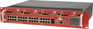
New R5560 |
14 |
125 |
128+6 |
rack mount 19 -2U |
60 |
2 |
max. 8k |
RJ45 |
basic PHA |
YES |
|
|
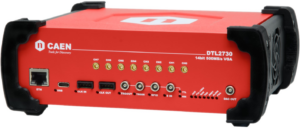
New DTL2730 |
14 |
500 |
8 |
Desktop |
TBD |
|
TBD |
MCX |
DPP-PHA(cs), DPP-PSD(cs), D-SCOPE(cs) |
YES |
|
|
V1761 |
10 |
4000 |
2 |
VME |
1000 |
1 |
7.2 M / 57.6 M |
MCX |
D-WAVE |
NO |
|
|
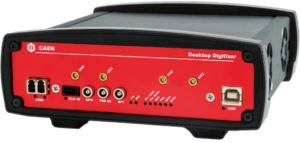
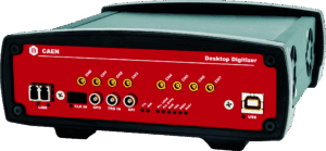
DT5751 |
10 |
2000(DES mode) - 1000 |
2(DES mode) - 4 |
Desktop |
500 |
0.2 / 1 |
3.6 M(DES mode) - 1.8 M |
MCX |
DPP-PSD, DPP-ZLEplus, D-WAVE |
NO |
|
|
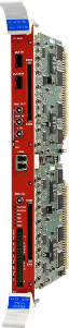
VX1740D |
12 |
62.5 |
64 |
VME64X |
30 |
2 / 10 |
192 k |
SMC 68P |
DPP-QDC, D-WAVE |
NO |
|
|
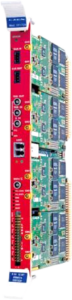
DT5725 / DT5725S |
14 |
250 |
8 |
Desktop |
125 |
0.5 - 2 |
640 k / 5.12 M |
MCX |
DPP-PHA, DPP-PSD, DPP-ZLEplus, DPP-DAW, D-WAVE |
NO |
|
|
VX1724 |
14 |
100 |
8 |
VME64X |
40 |
0.5 / 2.25 / 10 |
512 k / 4 M |
MCX |
DPP-PHA, DPP-DAW |
NO |
|
|
DT5761 |
10 |
4000 |
1 |
Desktop |
1000 |
1 |
7.2 M |
MCX |
D-WAVE |
NO |
|
|
VX2745 |
16 |
125 |
64 |
VME64X |
20 |
[0.04 ÷ 4] |
21 M |
2mm 40-pin header male |
D-SCOPE, DPP-PHA, DPP-PSD, DPP-ZLEplus<sup>(cs)</sup> |
YES |
|
|
DT5724 |
14 |
100 |
4 / 2 |
Desktop |
40 |
0.5 / 2.25 / 10 |
512 k / 4 M |
MCX |
DPP-PHA, DPP-DAW, D-WAVE |
NO |
|
|
DT5730 / DT5730S |
14 |
500 |
8 |
Desktop |
250 |
0.5 - 2 |
640 k / 5.12 M |
MCX |
DPP-PHA, DPP-PSD, DPP-ZLEplus, DPP-DAW, D-WAVE |
NO |
|
|
VX2740 |
16 |
125 |
64 |
VME64X |
50 |
2 |
21 M |
2mm 40-pin header male |
DPP-PHA, D-SCOPE, DPP-PSD, DPP-ZLEplus<sup>(cs)</sup> |
YES |
|
|
V1724 |
14 |
100 |
8 |
VME |
40 |
0.5 / 2.25 / 10 |
512 k / 4 M |
MCX |
DPP-PHA, DPP-DAW, D-WAVE |
NO |
|
|
VX1761 |
10 |
4000 |
2 |
VME64X |
1000 |
1 |
7.2 M / 57.6 M |
MCX |
D-SCOPE |
NO |
|
|
DT2740 |
16 |
125 |
64 |
Desktop |
50 |
2 |
21 M |
2mm 40-pin header male |
DPP-PHA, DPP-PSD, D-SCOPE, DPP-ZLEplus<sup>(cs)</sup> |
YES |
|
|
V2740 |
16 |
125 |
64 |
VME |
50 |
2 |
21 M |
2mm 40-pin header male |
DPP-PHA, DPP-PSD, D-SCOPE, DPP-ZLEplus<sup>(cs)</sup> |
YES |
|
|
New DT2751 |
14 |
1000 |
16 |
Desktop |
500 |
[0.2 ÷ 2] |
84 M |
MCX |
DPP-PHA, DPP-PSD, D-SCOPE<sup>(cs)</sup> |
YES |
|

|
V1730 / V1730S |
14 |
500 |
8 / 16 |
VME |
250 |
0.5 - 2 |
640 k / 5.12 M |
MCX |
DPP-PHA, DPP-PSD, DPP-ZLEplus, D-WAVE |
NO |
|
|
N6725 / N6725S |
14 |
250 |
8 |
NIM |
125 |
0.5 - 2 |
640 k / 5.12 M |
MCX |
DPP-PHA, DPP-PSD, DPP-ZLEplus, DPP-DAW, D-WAVE |
NO |
|
|
New VX2751 |
14 |
1000 |
16 |
VME64X |
500 |
[0.2 ÷ 2] |
84 M |
MCX |
DPP-PHA, DPP-PSD, D-SCOPE<sup>(cs)</sup> |
YES |
|
|
VX1740 |
12 |
62.5 |
64 |
VME64X |
30 |
2 / 10 |
192 k / 1.5 M |
SMC 68P |
D-WAVE |
NO |
|
|
DT5740D |
12 |
62.5 |
32(SMC conn.) - 16(MCX conn) |
Desktop |
30 |
2 / 10 |
192 k |
SMC 68P - MCX |
DPP-QDC,D-WAVE |
NO |
|
|
V2745 |
16 |
125 |
64 |
VME |
20 |
[0.04 ÷ 4] |
21 M |
2mm 40-pin header male |
DPP-PHA, DPP-PSD, D-SCOPE, DPP-ZLEplus<sup>(cs)</sup> |
YES |
|
|
DT5742 |
12 |
5000 (Based on DRS4 chip: 5 GS/s Switched Capacitor Array) |
16 + 1 |
Desktop |
500 |
1 |
0.128 / 1 |
MCX |
D-WAVE |
NO |
|
|
VX1725 / VX1725S |
14 |
250 |
8 / 16 |
VME64X |
125 |
0.5 - 2 |
640 k / 5.12 M |
MCX |
DPP-PHA, DPP-PSD, DPP-ZLEplus, DPP-DAW, D-WAVE |
NO |
|
|
VX1730 / VX1730S |
14 |
500 |
8 / 16 |
VME64X |
250 |
0.5 - 2 |
640 k / 5.12 M |
MCX |
DPP-PHA, DPP-PSD, DPP-ZLEplus, DPP-DAW, D-WAVE |
NO |
|
|
V2730B |
14 |
500 |
16 |
VME64 |
250 |
[0.2 ÷ 4] |
84 M |
MCX |
DPP-PHA, DPP-PSD, D-SCOPE(cs) |
YES |
|
|
N6730 / N6730S |
14 |
500 |
8 |
NIM |
250 |
0.5 - 2 |
640 k / 5.12 M |
MCX |
DPP-PHA, DPP-PSD, DPP-ZLEplus, DPP-DAW, D-WAVE |
NO |
|
|
V1743 |
12 |
3200 (Based on SAMLONG chip: 3.2 GS/s Switched Capacitor Array) |
16 |
VME |
500 |
2.5 |
0.007 M |
MCX |
D-WAVE |
NO |
|
|
VX1751 |
10 |
2000(DES mode) - 1000 |
2(DES mode) - 4 |
VME64X |
500 |
0.2 / 1 |
3.6 M(DES mode) - 1.8 M / 28.8 M(DES mode) - 14.4 M |
MCX |
DPP-PSD, DPP-ZLEplus, D-WAVE |
NO |
|
|
DT5740 |
12 |
62.5 |
32(SMC conn.) - 16(MCX conn) |
Desktop |
30 |
2 / 10 |
192 k |
SMC 68P - MCX |
D-WAVE |
NO |
|
|
V1720 |
12 |
250 |
8 |
VME |
125 |
2 |
1.25 M / 10 M |
MCX |
DPP-PSD, D-WAVE |
NO |
|
|
V1751 |
10 |
2000(DES mode) - 1000 |
2(DES mode) - 4 |
VME |
500 |
0.2 / 1 |
3.6 M(DES mode) - 1.8 M / 28.8 M(DES mode) - 14.4 M |
MCX |
DPP-PSD, DPP-ZLEplus, D-WAVE |
NO |
|
|
VX1742 |
12 |
5000 (Based on DRS4 chip: 5 GS/s Switched Capacitor Array) |
32 + 2 |
VME64X |
500 |
1 |
0.128 / 1 |
MCX |
D-WAVE |
NO |
|
|
DT5743 |
12 |
3200 (Based on SAMLONG chip: 3.2 GS/s Switched Capacitor Array) |
8 |
Desktop |
500 |
2.5 |
0.007 M |
MCX |
D-WAVE |
NO |
|
|
DT5720 |
12 |
250 |
4 / 2 |
Desktop |
125 |
2 |
1.25 M / 10 M |
MCX |
DPP-PSD, D-WAVE |
NO |
|
|
V1742 |
12 |
5000 (Based on DRS4 chip: 5 GS/s Switched Capacitor Array) |
32 + 2 |
VME |
500 |
1 |
0.128 / 1 |
MCX |
D-WAVE |
NO |
|
|
DT2730 |
14 |
500 |
32 / 16 |
Desktop |
250 |
[0.2 ÷ 4] |
84 M |
MCX |
DPP-PHA, DPP-PSD, D-SCOPE |
YES |
|
|
VX1743 |
12 |
3200 (Based on SAMLONG chip: 3.2 GS/s Switched Capacitor Array) |
16 |
VME64X |
500 |
2.5 |
0.007 M |
MCX |
D-WAVE |
NO |
|
|
V1740D |
12 |
62.5 |
64 |
VME |
30 |
2 / 10 |
192 k |
SMC 68P |
DPP-QDC, D-WAVE |
NO |
|
|
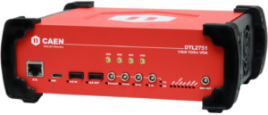
New DTL2751 |
14 |
1000 |
4 |
Desktop |
TBD |
TBD |
TBD |
MCX |
DPP-PSD(cs), D-SCOPE(cs) |
YES |
|
|
VX1720 |
12 |
250 |
8 |
VME64X |
125 |
2 |
1.25 M / 10 M |
MCX |
DPP-PSD, D-WAVE |
NO |
|
|
N6742 |
12 |
5000 (Based on DRS4 chip: 5 GS/s Switched Capacitor Array) |
16 + 1 |
NIM |
500 |
1 |
0.128 / 1 |
MCX |
D-WAVE |
NO |
Technical Specifications
|
Package |
Form Factor: 1-unit wide NIM module |
|
Analog Input |
|
|
Digital Conversion |
|
|
System Performance |
ENOB:
SINAD: THD: 11.20 (48 kS Buffer)
69.20 dB 87.10 dB SFDR:
SIGMA: 94.9 dB
0.50 LSB rms (48 kS Buffer, open input) |
|
ADC Sampling Clock generation |
Supports three operating modes:
|
|
Digital I/O |
|
|
Memory Buffer |
|
|
Common Trigger |
|
|
Trigger Time Stamp |
31-bit counter, 16 ns resolution, 17 s range(*) |
|
ADC and Memory controller FPGA |
One Altera Cyclone EP3C40 per 16 channel |
|
Multi Modules Synchronization |
|
|
Optical Link |
CAEN CONET proprietary protocol Up to 80 MB/s transfer rate |
|
USB interface |
|
|
Upgrade |
Firmware can be upgraded via Optical Link or USB interface |
|
Software |
|
Footer