
-
10 bit @ 4 GS/s
-
Analog input on MCX coaxial connector (50 Ω, single ended)
-
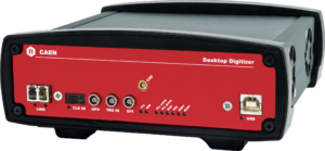
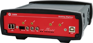
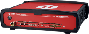
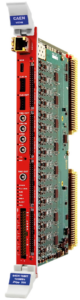
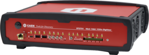
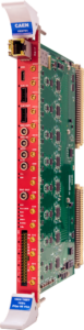
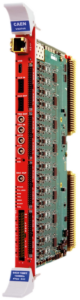
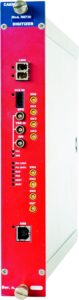
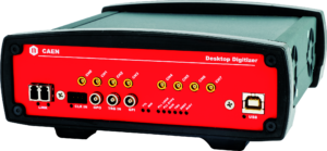
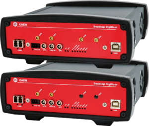
1 channel, Desktop module
-
1 Vpp input dynamic range with programmable DC offset adjustment
-
Time-stamped Waveform Recorder
-
Memory buffer: 7.2 MS/ch
-
Programmable event size and post-trigger adjustment
-
USB and Optical Link communication interfaces
-
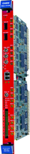
Multi-board synchronization features
-
Daisy chain capability
-
Compliant with CAEN WaveDump, C and LabVIEW Libraries
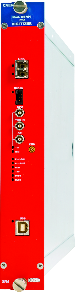
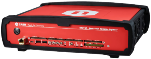
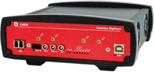
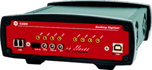
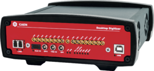
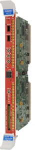
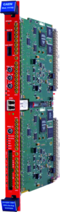
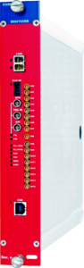
The N6761 is the CAEN Waveform Digitizer with the highest sampling rate Flash ADC (10 bit @ 4GS/s).
It can record fast signals from fast organic, inorganic and liquid scintillators coupled to PMTs or Silicon Photomultipliers, Diamond detectors and others, and save them with high efficiency and precision for offline advanced timing analysis. The acquisition can be externally vetoed/gated. Multiple boards can be synchronized to build up complex systems.
The data stream is written in a circular memory buffer with independent read/write access, which reduces the dead-time of the acquisition process.
The acquisition is fully controlled by CAEN WaveDump software, which manages the settings, plots and saves the waveforms. Libraries and demo software in C and LabView are available for integration and customization of specific acquisition systems.
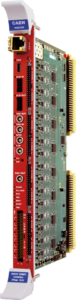
The N6761 comes in a NIM form factor with 1 input channel. The communication to and from the board is provided through USB and Optical Link interfaces.
Accessories
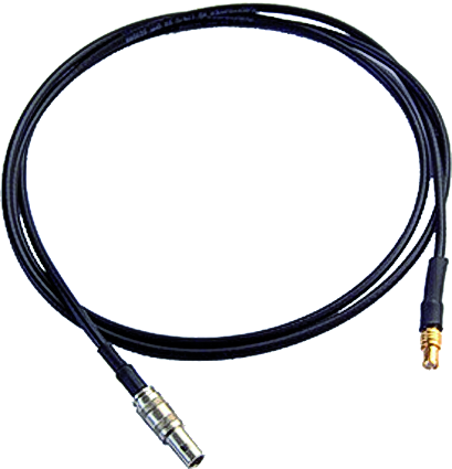
A318
A317
AI2700
A654
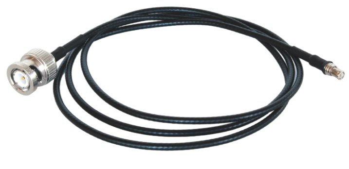
A659
You also may be interested in…
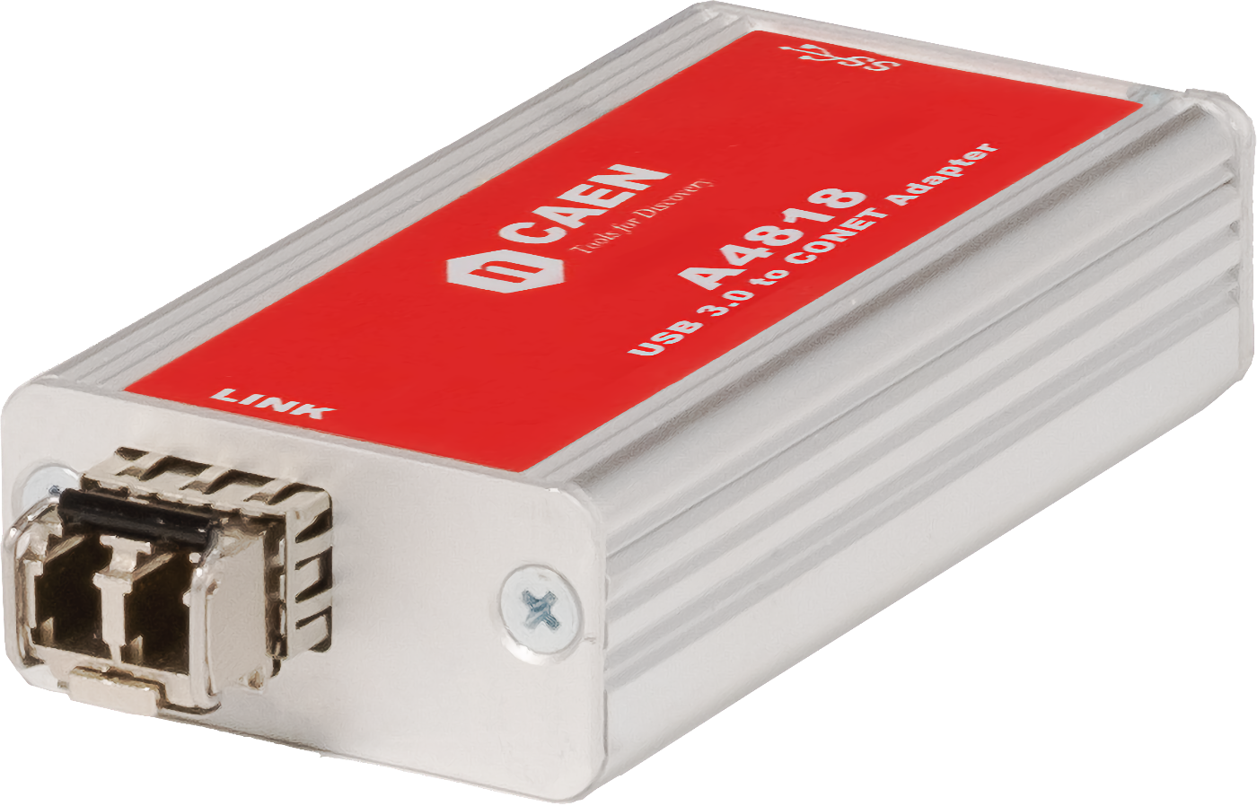
A4818
NIM8301
NIM8302
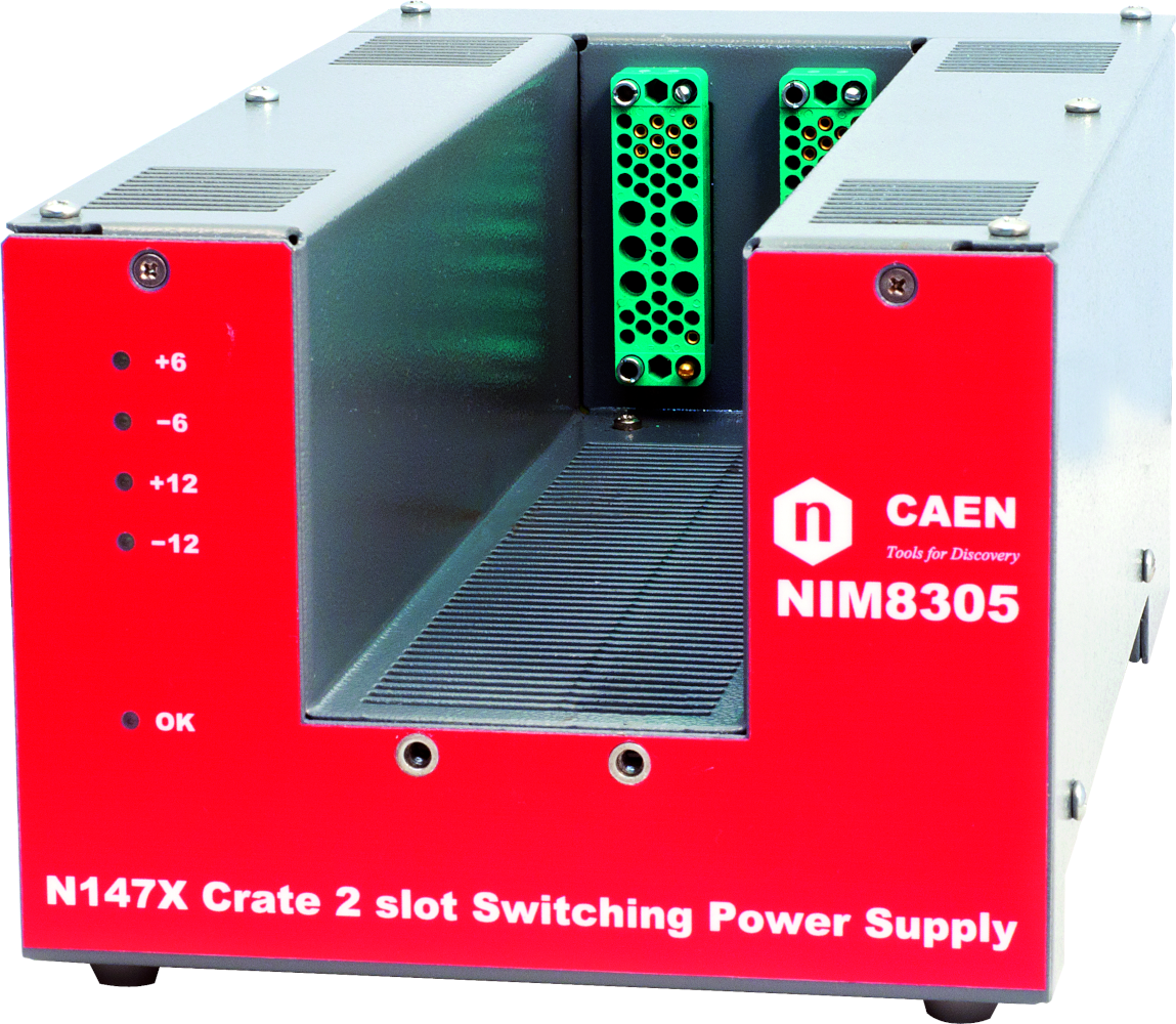
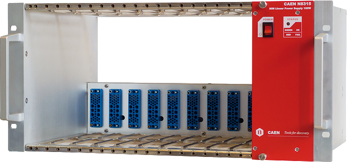
NIM8305
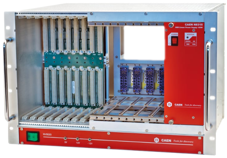
NV8020A
NIM8303
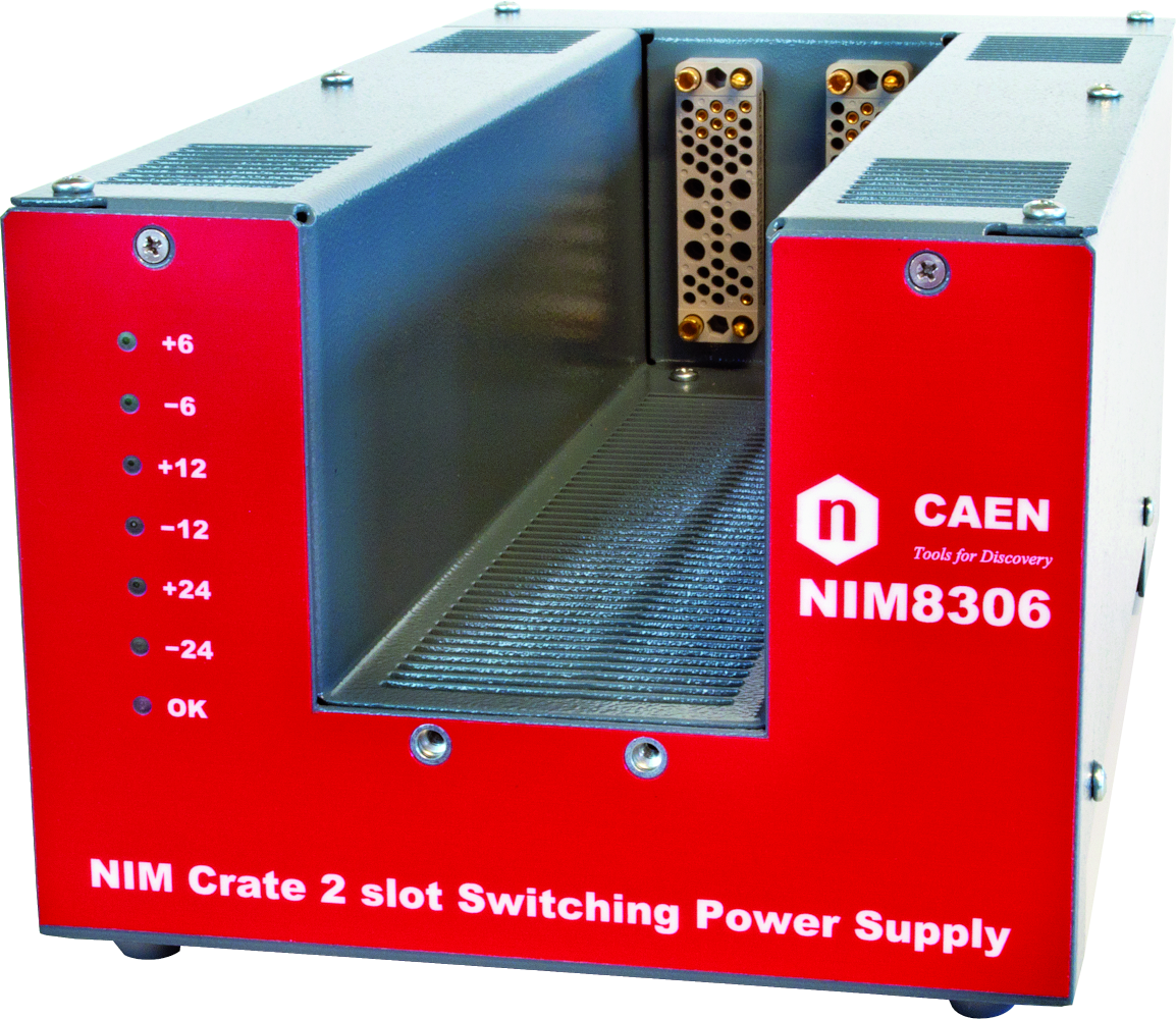
NIM8306
A5818
NIM8304
Request a Quote

Compare

|
Image
|
Name
|
Package
|
No. of Channels
|
Max Sampling Rate (MS/s)
|
Bandwidth (MHz)
|
Full Scale Range (V)
|
Resolution (bits)
|
Board Memory (Samples/ch)
|
Analog Input Connectors
|
CAEN firmware
|
Open FPGA
|
|
|
VX2730 |
VME64X |
32 |
500 |
250 |
[0.2 ÷ 4] |
14 |
84 M |
MCX |
DPP-PHA, DPP-PSD, D-SCOPE<sup>(cs)</sup> |
YES |
|
|
V1725 / V1725S |
VME |
8 / 16 |
250 |
125 |
0.5 - 2 |
14 |
640 k / 5.12 M |
MCX |
DPP-PHA, DPP-PSD, DPP-ZLEplus, D-WAVE |
NO |
|
|
DT2745 |
Desktop |
64 |
125 |
20 |
[0.04 + 4] |
16 |
21 M |
2mm 40-pin header male |
DPP-PHA, DPP-PSD, D-SCOPE, DPP-ZLEplus<sup>(cs)</sup> |
YES |
|
|
New R5560 |
rack mount 19 -2U |
128+6 |
125 |
60 |
2 |
14 |
max. 8k |
RJ45 |
n. a. |
YES |
|
|
New DTL2730 |
Desktop |
8 |
500 |
TBD |
TBD |
14 |
TBD |
MCX |
DPP-PHA(cs), DPP-PSD(cs), D-SCOPE(cs) |
YES |
|
|
V1761 |
VME |
2 |
4000 |
1000 |
1 |
10 |
7.2 M / 57.6 M |
MCX |
D-WAVE |
NO |
|
|
DT5751 |
Desktop |
2(DES mode) - 4 |
2000(DES mode) - 1000 |
500 |
0.2 / 1 |
10 |
3.6 M(DES mode) - 1.8 M |
MCX |
DPP-PSD, DPP-ZLEplus, D-WAVE |
NO |
|

|
VX1740D |
VME64X |
64 |
62.5 |
30 |
2 / 10 |
12 |
192 k |
SMC 68P |
DPP-QDC, D-WAVE |
NO |
|
|
DT5725 / DT5725S |
Desktop |
8 |
250 |
125 |
0.5 - 2 |
14 |
640 k / 5.12 M |
MCX |
DPP-PHA, DPP-PSD, DPP-ZLEplus, DPP-DAW, D-WAVE |
NO |
|
|
VX1724 |
VME64X |
8 |
100 |
40 |
0.5 / 2.25 / 10 |
14 |
512 k / 4 M |
MCX |
DPP-PHA, DPP-DAW |
NO |
|
|
DT5761 |
Desktop |
1 |
4000 |
1000 |
1 |
10 |
7.2 M |
MCX |
D-WAVE |
NO |
|
|
VX2745 |
VME64X |
64 |
125 |
20 |
[0.4 ÷ 4] |
16 |
21 M |
2mm 40-pin header male |
D-SCOPE, DPP-PHA, DPP-PSD, DPP-ZLEplus<sup>(cs)</sup> |
YES |
|
|
DT5724 |
Desktop |
4 / 2 |
100 |
40 |
0.5 / 2.25 / 10 |
14 |
512 k / 4 M |
MCX |
DPP-PHA, DPP-DAW, D-WAVE |
NO |
|
|
DT5730 / DT5730S |
Desktop |
8 |
500 |
250 |
0.5 - 2 |
14 |
640 k / 5.12 M |
MCX |
DPP-PHA, DPP-PSD, DPP-ZLEplus, DPP-DAW, D-WAVE |
NO |
|
|
VX2740 |
VME64X |
64 |
125 |
50 |
2 |
16 |
21 M |
2mm 40-pin header male |
DPP-PHA, D-SCOPE, DPP-PSD, DPP-ZLEplus<sup>(cs)</sup> |
YES |
|
|
V1724 |
VME |
8 |
100 |
40 |
0.5 / 2.25 / 10 |
14 |
512 k / 4 M |
MCX |
DPP-PHA, DPP-DAW, D-WAVE |
NO |
|
|
VX1761 |
VME64X |
2 |
4000 |
1000 |
1 |
10 |
7.2 M / 57.6 M |
MCX |
D-SCOPE |
NO |
|
|
DT2740 |
Desktop |
64 |
125 |
50 |
2 |
16 |
21 M |
2mm 40-pin header male |
DPP-PHA, DPP-PSD, D-SCOPE, DPP-ZLEplus<sup>(cs)</sup> |
YES |
|
|
V2740 |
VME |
64 |
125 |
50 |
2 |
16 |
21 M |
2mm 40-pin header male |
DPP-PHA, DPP-PSD, D-SCOPE, DPP-ZLEplus<sup>(cs)</sup> |
YES |
|
|
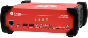
New DT2751 |
Desktop |
16 |
1000 |
500 |
[0.2 ÷ 2] |
14 |
84 M |
MCX |
DPP-PHA, DPP-PSD, D-SCOPE<sup>(cs)</sup> |
YES |
|
|
V1730 / V1730S |
VME |
8 / 16 |
500 |
250 |
0.5 - 2 |
14 |
640 k / 5.12 M |
MCX |
DPP-PHA, DPP-PSD, DPP-ZLEplus, D-WAVE |
NO |
|
|
N6725 / N6725S |
NIM |
8 |
250 |
125 |
0.5 - 2 |
14 |
640 k / 5.12 M |
MCX |
DPP-PHA, DPP-PSD, DPP-ZLEplus, DPP-DAW, D-WAVE |
NO |
|
|
New VX2751 |
VME64X |
16 |
1000 |
500 |
[0.2 ÷ 2] |
14 |
84 M |
MCX |
DPP-PHA, DPP-PSD, D-SCOPE<sup>(cs)</sup> |
YES |
|
|
VX1740 |
VME64X |
64 |
62.5 |
30 |
2 / 10 |
12 |
192 k / 1.5 M |
SMC 68P |
D-WAVE |
NO |
|
|
DT5740D |
Desktop |
32(SMC conn.) - 16(MCX conn) |
62.5 |
30 |
2 / 10 |
12 |
192 k |
SMC 68P - MCX |
DPP-QDC,D-WAVE |
NO |
|
|
V2745 |
VME |
64 |
125 |
20 |
[0.04 + 4] |
16 |
21 M |
2mm 40-pin header male |
DPP-PHA, DPP-PSD, D-SCOPE, DPP-ZLEplus<sup>(cs)</sup> |
YES |
|
|
DT5742 |
Desktop |
16 + 1 |
5000 (Based on DRS4 chip: 5 GS/s Switched Capacitor Array) |
500 |
1 |
12 |
0.128 / 1 |
MCX |
D-WAVE |
NO |
|
|
VX1725 / VX1725S |
VME64X |
8 / 16 |
250 |
125 |
0.5 - 2 |
14 |
640 k / 5.12 M |
MCX |
DPP-PHA, DPP-PSD, DPP-ZLEplus, DPP-DAW, D-WAVE |
NO |
|
|
VX1730 / VX1730S |
VME64X |
8 / 16 |
500 |
250 |
0.5 - 2 |
14 |
640 k / 5.12 M |
MCX |
DPP-PHA, DPP-PSD, DPP-ZLEplus, DPP-DAW, D-WAVE |
NO |
|
|
V2730B |
VME64 |
16 |
500 |
250 |
[0.2 ÷ 4] |
14 |
MCX |
84 M |
DPP-PHA, DPP-PSD, D-SCOPE(cs) |
YES |
|
|
N6730 / N6730S |
NIM |
8 |
500 |
250 |
0.5 - 2 |
14 |
640 k / 5.12 M |
MCX |
DPP-PHA, DPP-PSD, DPP-ZLEplus, DPP-DAW, D-WAVE |
NO |
|
|
V1743 |
VME |
16 |
3200 (Based on SAMLONG chip: 3.2 GS/s Switched Capacitor Array) |
500 |
2.5 |
12 |
0.007 M |
MCX |
D-WAVE |
NO |
|
|
VX1751 |
VME64X |
2(DES mode) - 4 |
2000(DES mode) - 1000 |
500 |
0.2 / 1 |
10 |
3.6 M(DES mode) - 1.8 M / 28.8 M(DES mode) - 14.4 M |
MCX |
DPP-PSD, DPP-ZLEplus, D-WAVE |
NO |
|

|
DT5740 |
Desktop |
32(SMC conn.) - 16(MCX conn) |
62.5 |
30 |
2 / 10 |
12 |
192 k |
SMC 68P - MCX |
D-WAVE |
NO |
|
|
V1720 |
VME |
8 |
250 |
125 |
2 |
12 |
1.25 M / 10 M |
MCX |
DPP-PSD, D-WAVE |
NO |
|
|
V1751 |
VME |
2(DES mode) - 4 |
2000(DES mode) - 1000 |
500 |
0.2 / 1 |
10 |
3.6 M(DES mode) - 1.8 M / 28.8 M(DES mode) - 14.4 M |
MCX |
DPP-PSD, DPP-ZLEplus, D-WAVE |
NO |
|
|
VX1742 |
VME64X |
32 + 2 |
5000 (Based on DRS4 chip: 5 GS/s Switched Capacitor Array) |
500 |
1 |
12 |
0.128 / 1 |
MCX |
D-WAVE |
NO |
|
|
DT5743 |
Desktop |
8 |
3200 (Based on SAMLONG chip: 3.2 GS/s Switched Capacitor Array) |
500 |
2.5 |
12 |
0.007 M |
MCX |
D-WAVE |
NO |
|
|
DT5720 |
Desktop |
4 / 2 |
250 |
125 |
2 |
12 |
1.25 M / 10 M |
MCX |
DPP-PSD, D-WAVE |
NO |
|
|
V1742 |
VME |
32 + 2 |
5000 (Based on DRS4 chip: 5 GS/s Switched Capacitor Array) |
500 |
1 |
12 |
0.128 / 1 |
MCX |
D-WAVE |
NO |
|
|
DT2730 |
Desktop |
32 / 16 |
500 |
250 |
[0.2 ÷ 4] |
14 |
MCX |
84 M |
DPP-PHA, DPP-PSD, D-SCOPE |
YES |
|
|
VX1743 |
VME64X |
16 |
3200 (Based on SAMLONG chip: 3.2 GS/s Switched Capacitor Array) |
500 |
2.5 |
12 |
0.007 M |
MCX |
D-WAVE |
NO |
|
|
V1740D |
VME |
64 |
62.5 |
30 |
2 / 10 |
12 |
192 k |
SMC 68P |
DPP-QDC, D-WAVE |
NO |
|
|
New DTL2751 |
Desktop |
4 |
1000 |
TBD |
TBD |
14 |
MCX |
TBD |
DPP-PSD(cs), D-SCOPE(cs) |
YES |
|
|
VX1720 |
VME64X |
8 |
250 |
125 |
2 |
12 |
1.25 M / 10 M |
MCX |
DPP-PSD, D-WAVE |
NO |
|
|
N6742 |
NIM |
16 + 1 |
5000 (Based on DRS4 chip: 5 GS/s Switched Capacitor Array) |
500 |
1 |
12 |
0.128 / 1 |
MCX |
D-WAVE |
NO |
Technical Specifications
|
GENERAL |
Form Factor: 1-unit wide NIM |
|
ANALOG INPUT |
|
|
DIGITAL CONVERSION |
|
|
ADC Clock Generation |
|
|
DIGITAL I/O |
CLK-IN (AMP Modu II) GPO (LEMO) TRG-IN (LEMO) |
|
ACQUISITION MEMORY |
|
|
TRIGGER |
Trigger Source Trigger Time Stamp |
|
SYNCHRONIZATION |
Clock Propagation Acquisition Synchronization Trigger Time Stamp Alignment |
|
ADC & Memory Controller FPGA |
Two Altera Cyclone III EP3C16 |
|
COMMUNICATION INTERFACE |
USB: USB 2.0 compliant Transfer rate up to 30 MB/s |
|
FIRMWARE |
Waveform Recording Firmware: Free firmware for waveform recording |
|
SOFTWARE |
Libraries: General purpose C and LabVIEW Libraries |
|
POWER CONSUMPTIONS |
3.9 A @ +6 V |
Footer